ESD protection device

a protection device and integrated circuit technology, applied in the direction of solid-state devices, resistors, basic electric elements, etc., can solve the problems of degrading the performance of the ggnmos device, secondary breakdown, or snapping, and the analog performance of the pin degrade in the state of the art cmos technology,

Inactive Publication Date: 2005-08-30
CHARTERED SEMICONDUCTOR MANUFACTURING +1
View PDF9 Cites 36 Cited by
  • Summary
  • Abstract
  • Description
  • Claims
  • Application Information

AI Technical Summary

Benefits of technology

[0010]A yet further object of the present invention is to provide a device having excellent ESD performance in a state of the art CMOS process without requiring a large area or adding excessive parasitic capacitance.
[0011]A yet further object of the present invention is to provide a device that can be used in multiple configurations.

Problems solved by technology

Designing electrostatic discharge (ESD) protection structures for high-speed analog or radio frequency (RF) applications presents many challenges.
These challenges are due to the stringent requirements for low input impedance and to the need to keep the area of the input protection devices to a minimum.
This, in turn, degrades the analog performance of the pin 14.
In addition, it is found that the secondary breakdown, or snap-back, performance of the GGNMOS device 10 is degraded in state of the art CMOS technologies.

Method used


Image

  • ESD protection device
  • ESD protection device
  • ESD protection device

Examples


Embodiment Construction

[0027]The preferred embodiments of the present invention disclose a novel integrated circuit device and a method to manufacture this a device. The device is called a PIN diode gated, MOSFET. This new device is particularly useful as an ESD protection device. Two methods for using this device for ESD protection are disclosed. It should be clear to those experienced in the art that the present invention can be applied and extended without deviating from the scope of the present invention.

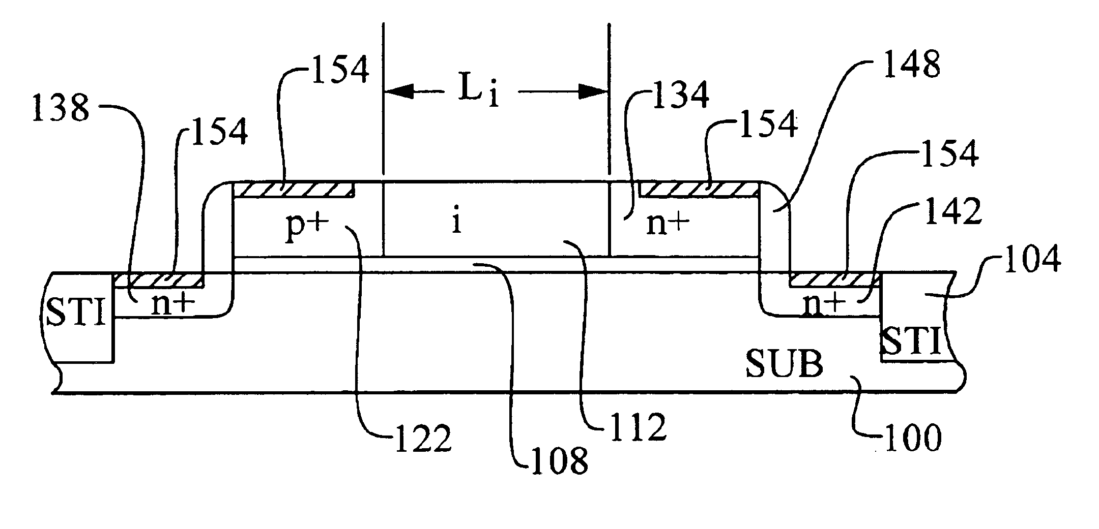
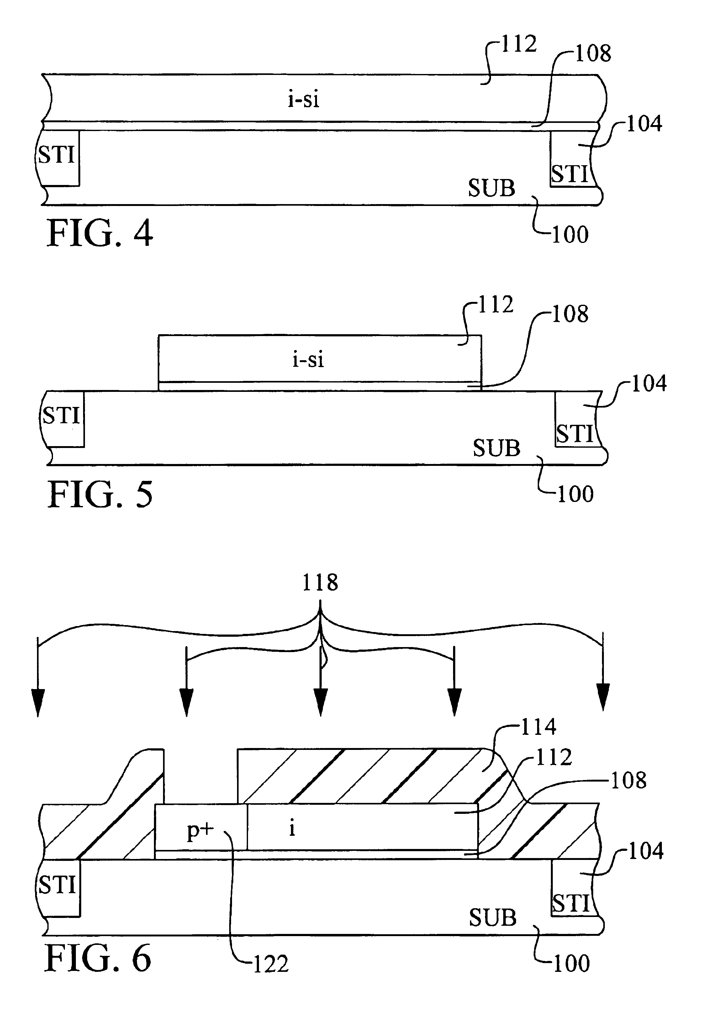
[0028]Referring now to FIGS. 4 through 10, the preferred embodiment of the present invention is illustrated, and, more particularly, the preferred method to form a PIN diode gated, MOSFET device is illustrated. Several important features of the present invention are shown herein and are discussed below. This embodiment discloses a method to form a PIN diode gated, MOSFET device. In particular, an NMOS device is illustrated. However, the types of the various doped regions could be altered to create a P...


PUM


Abstract

A new method to form an integrated circuit device is achieved. The method comprises forming a dielectric layer overlying a semiconductor substrate. An intrinsic semiconductor layer is formed overlying the dielectric layer. The intrinsic semiconductor layer is patterned. A p+ region is formed in the intrinsic semiconductor layer. An n+ region is formed in the intrinsic semiconductor layer. The p+ region and said n+ region are laterally separated by an intrinsic region to thereby form a PIN diode device. A source region and a drain region are formed in the semiconductor substrate to thereby complete a MOSFET device. The PIN diode device is a gate electrode for the MOSFET device.

Description

BACKGROUND OF THE INVENTION[0001](1) Field of the Invention[0002]The invention relates to an integrated circuit device and, more particularly, to a device for protecting an integrated circuit from electrostatic discharge.[0003](2) Description of the Prior Art[0004]Designing electrostatic discharge (ESD) protection structures for high-speed analog or radio frequency (RF) applications presents many challenges. These challenges are due to the stringent requirements for low input impedance and to the need to keep the area of the input protection devices to a minimum. Referring now to FIG. 1, a prior art ESD protection circuit is shown. In this traditional approach, a grounded gate NMOS (GGNMOS) device 10 is used. The gate of the device is connected to the grounded pin or pad 18. During an ESD event on the input pin 14, the parasitic bipolar device formed by the source, bulk, and drain (n-p-n) conducts current away from the input pin 14 to the ground pin 18 due to reverse junction breakd...

Claims


Application Information

Patent Timeline
Patent Type & Authority Patents(United States)
IPC IPC(8): H01L21/02H01L21/70H01L21/425H01L23/58H01L23/62H01L21/8234H01L31/06H01L31/075H01L27/02H01L29/49H01L29/868
CPCH01L27/0255H01L27/0266H01L29/4983H01L29/868H01L2924/0002H01L2924/00Y02E10/548
Inventor MANNA, INDRAJITLO, KENG FOOTAN, PEE YAFILIPPI, RAYMOND
Owner CHARTERED SEMICONDUCTOR MANUFACTURING
Why Eureka
Try Eureka