Process for encapsulating a component made of organic semiconductors

a technology of organic semiconductors and components, applied in the direction of discharge tube luminescnet screens, soldering devices, manufacturing tools, etc., can solve the problems of premature failure of oleds, and achieve the effects of good sealing, long life time and good sealing

Inactive Publication Date: 2005-08-30
PATENT TREUHAND GES GMBH
View PDF22 Cites 77 Cited by
  • Summary
  • Abstract
  • Description
  • Claims
  • Application Information

AI Technical Summary

Benefits of technology

[0004]It is an object of the invention to provide a process for encapsulating a component made of organic semiconductors with a good seal....

Problems solved by technology

However, organic adhesives of this nature do not achieve a satisfactory seal ...

Method used


Image

  • Process for encapsulating a component made of organic semiconductors
  • Process for encapsulating a component made of organic semiconductors

Examples


Embodiment Construction

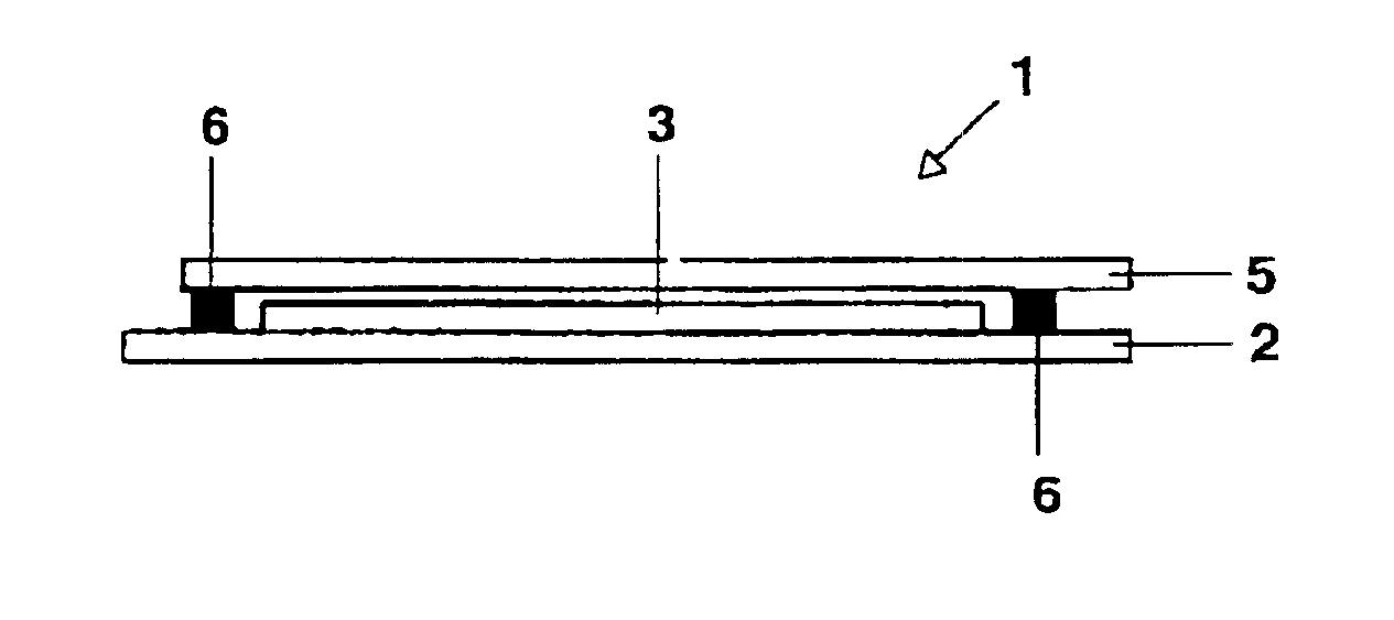
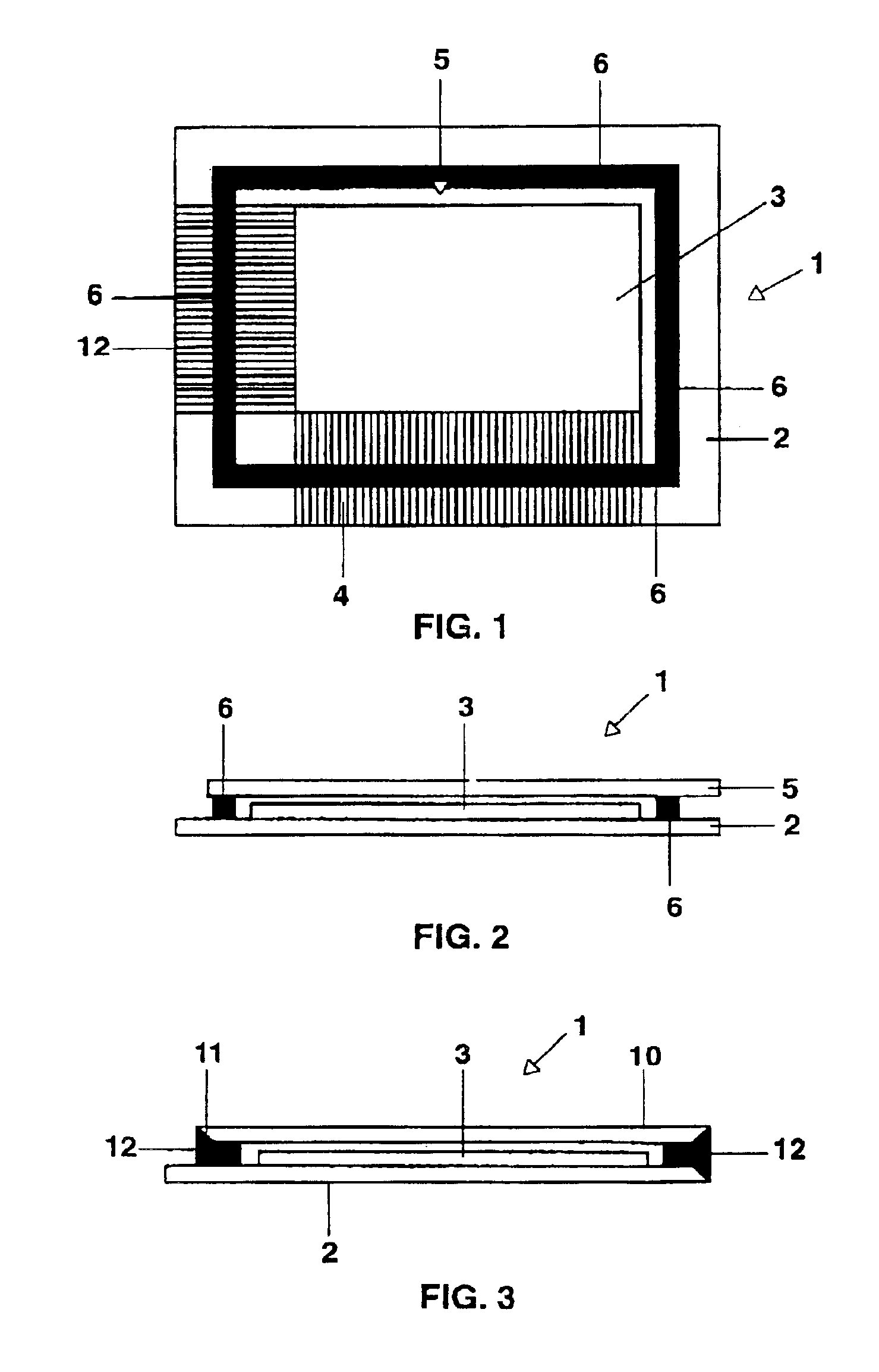
[0009]Organic LEDs (OLEDS), and in particular displays composed of organic LEDs, comprise a layer assembly of organic layers (the actual OLED) and metallic layers for contact-making (electrodes) which are positioned between two thin sheets of glass (e.g. 0.5 to 1.0 mm thick). These form the base (substrate) and the cover of a housing. Furthermore, if appropriate, the housing may also have side walls. Without encapsulation, these layers would be attacked by oxygen and water vapor, leading to the failure of the OLED.

[0010]An encapsulation process for the OLED which permanently mechanically joins the remaining parts of the housing to the substrate and surrounds the OLED in a gas-tight manner, thus protecting it from attack by oxygen and moisture, has been developed. The OLED must not be damaged by excessive thermal loading during the closure operation.

[0011]A method for mechanically stably joining the substrate and remaining housing parts made from glass, between which the OLED is situ...


PUM

PropertyMeasurementUnit
Nanoscale particle sizeaaaaaaaaaa
Wavelengthaaaaaaaaaa
Semiconductor propertiesaaaaaaaaaa

Abstract

A process for encapsulating a component made of organic semiconductors is provided which includes steps of: a) providing a housing including a substrate with electrical connections and a cover; b) mixing a soldering glass with at least one of a binder and a solvent; c) applying the soldering glass at least to the cover, in the form of an encircling bank; d) expelling the binder or solvent; e) sintering-on of the solder; f) covering the substrate with layers which represent the semiconductor component together with electrodes; g) placing the cover onto the substrate; and h) locally heating the soldering glass by means of a light source with a predetermined peak wavelength, wherein the housing parts and soldering glass are matched to one another such that their coefficients of thermal expansion differ from one another by less than 1.0×10⁻⁶K−1.

Description

FIELD OF THE INVENTION[0001]The invention relates to a process for encapsulating a component made of organic semiconductors such as OLEDs, i.e. organic light-emitting devices based on electroluminescence.BACKGROUND ART[0002]WO 01 / 18 887 has already disclosed a process for encapsulating a component made of organic semiconductors, comprising a transparent substrate, an electrode which has been applied to it, luminescent layers of different colors and a counterelectrode. The semiconductor component is encapsulated in an airtight manner by means of a housing which is joined to the substrate by adhesive.[0003]The adhesive used is an UV-curable reaction adhesive based on epoxy resin. However, organic adhesives of this nature do not achieve a satisfactory seal with respect to oxygen and moisture, which leads to premature failure of the OLEDs.OBJECTS OF THE INVENTION[0004]It is an object of the invention to provide a process for encapsulating a component made of organic semiconductors with ...

Claims


Application Information

Patent Timeline
IPC IPC(8): H01L51/52H01L51/50H05B33/04H05B33/10
CPCH01L51/5246H10K59/873H10K50/8426
Inventor LANGER, ALFREDMESSNER, EKKEHARD
Owner PATENT TREUHAND GES GMBH
Why Eureka
Try Eureka