Semiconductor memory device with reduced data access time

a memory device and memory technology, applied in the field of semiconductor memory devices, can solve the problems of small amount of charges stored in the capacitors, many problems may arise, and the operation speed of the memory device is slower

Active Publication Date: 2005-08-30
SK HYNIX INC
View PDF17 Cites 163 Cited by
  • Summary
  • Abstract
  • Description
  • Claims
  • Application Information

AI Technical Summary

Benefits of technology

[0055]It is, therefore, an object of the present invention to provide a method and an apparatus of a memory device for accessing data on high speed so that the data restoration time does not affect seriously the data access time.

Problems solved by technology

As a result, many problems may arise because the operation speed of the memory device is slower than that of CPU.
Furthermore, since a small amount of charges stored in the capacitor may be lost with lapse of time, the memory device needs a refresh operation for periodically recharging the capacitor.
As a result, if the charge stored in the capacitor is not amplified periodically, the charge stored in the capacitor may be lost to thereby allow the stored data to be corrupted.
However, as mentioned above, it is difficult to apply the bank interleaving mode in the intra bank data access of the conventional memory device and, to obtain higher data access time in the convention memory device.
If a system uses the conventional memory device whose data access speed is seriously affected by the data access pattern, there may be occurred some critical problems about the operation reliability of the system because the operation speed of the system may not be stable.

Method used


Image

  • Semiconductor memory device with reduced data access time
  • Semiconductor memory device with reduced data access time
  • Semiconductor memory device with reduced data access time

Examples


Embodiment Construction

[0103]Hereinafter, a semiconductor memory device in accordance with the present invention will be described in detail referring to the accompanying drawings.

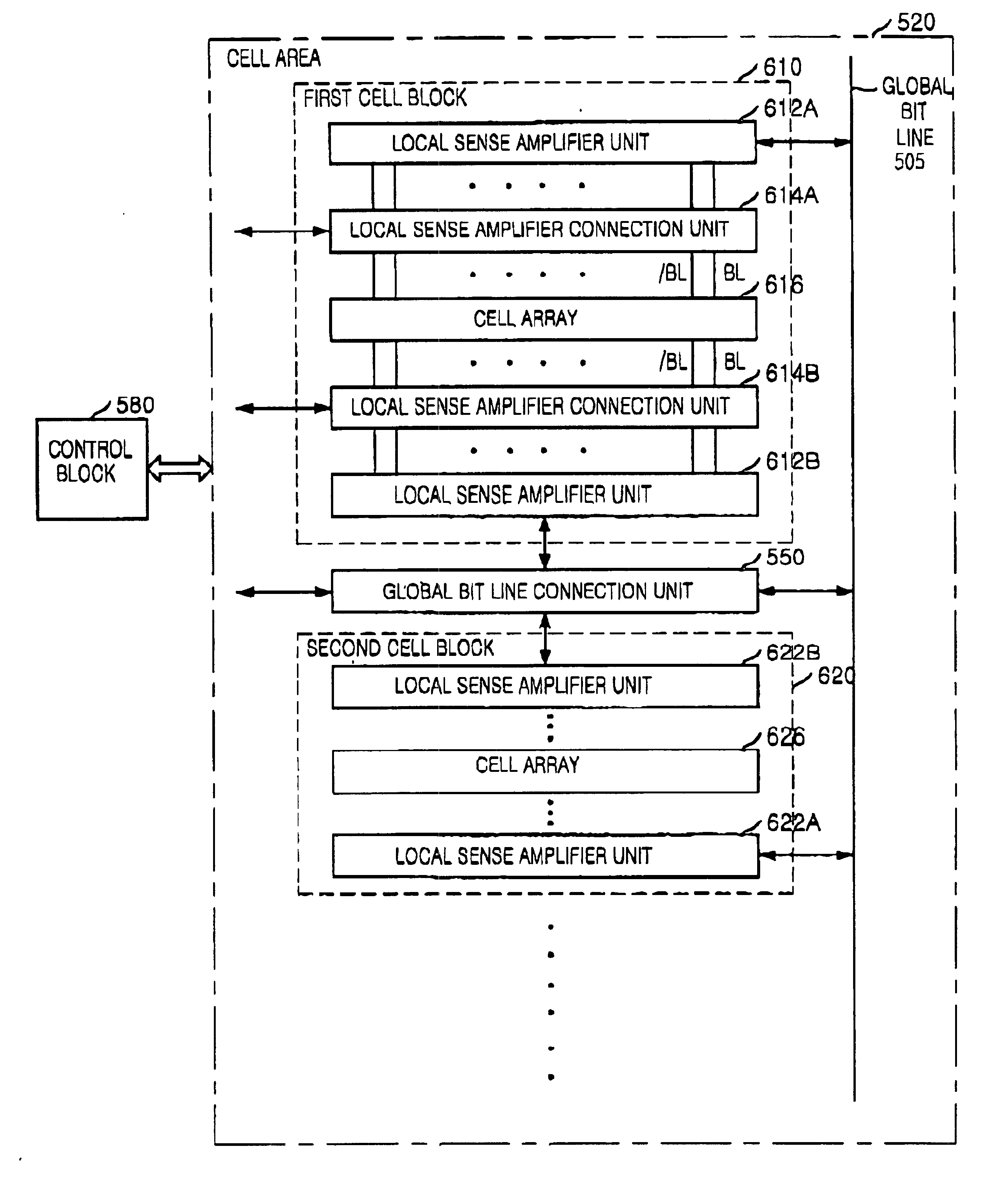
[0104]Referring to FIG. 5, there is shown a block diagram showing a semiconductor memory device in accordance with a preferred embodiment of the present invention.

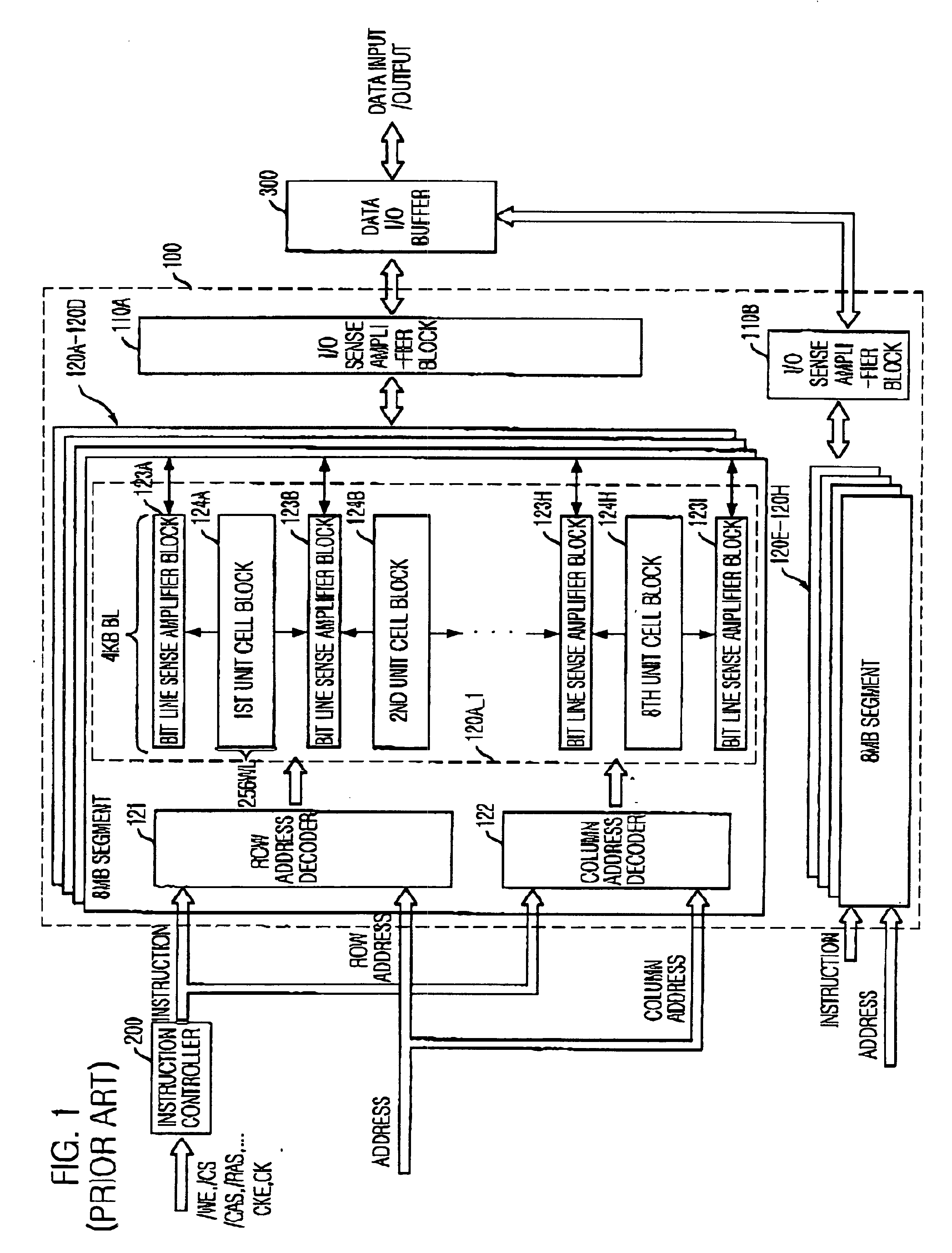
[0105]As shown, the semiconductor memory device includes a plurality of banks. Each bank has at least one segment 510A to 510D and an input / output (I / O) sense amplifier block 590. The segment, e.g., 510A, includes a cell area 520, a control block 580, a row address decoder 560 and a column address decoder 565. Herein, because the row and column address decoder 560 and 565 are similar to those of the conventional memory device as shown in FIG. 1, detailed descriptions about operation of the row and column address decoder 560 and 565 is omitted for the sake of convenience.

[0106]Referring to FIG. 6, the cell area 520 includes at least two cell blocks, e.g., 610 and 620, a...


PUM


Abstract

A memory device includes at least two cell blocks connected to a global bit line for outputting data in response to an instruction; at least one global bit line connection unit for selectively connecting the global bit line to each cell block under control of a control block, one global bit line connection unit being allocated between the two cell blocks; and said control block for controlling output of data stored in each cell block to the global bit line and restoration of the outputted data of the global bit line to the original cell block or another cell block which is determined by depending upon whether data in response to a next instruction is outputted from the original cell block or another cell block.

Description

FIELD OF THE INVENTION[0001]The present invention relates to a semiconductor memory device; and, more particularly, to the semiconductor memory device capable of providing a reduced data access time.DESCRIPTION OF RELATED ART[0002]Generally, a semiconductor memory device is classified as a random access memory (RAM) and a read only memory (ROM).[0003]The RAM includes a Dynamic RAM (DRAM) and a Static RAM (SRAM). One cell of the dynamic RAM has one transistor and one capacitor and that of the static RAM does four transistors and two load resistances. The DRAM is used more widespread than the SRAM because the DRAM is more efficient than SRAM in a chip integration and a manufacturing process.[0004]Today, an operation speed of a central processing unit (CPU) is more dramatically advanced than that of the DRAM. As a result, many problems may arise because the operation speed of the memory device is slower than that of CPU. For overcoming these problems, several kinds of scheme in the mem...

Claims


Application Information

Patent Timeline
Patent Type & Authority Patents(United States)
IPC IPC(8): G11C7/18G11C11/408G11C7/00G11C11/4097G11C11/409G11C11/407G11C11/401
CPCG11C7/18G11C11/4097G11C11/4087G11C11/401
Inventor AHN, JIN-HONGHONG, SANG-HOONKIM, SE-JUNKO, JAE-BUM
Owner SK HYNIX INC
Why Eureka
Try Eureka