Inspection equipment

a technology of inspection equipment and equipment, applied in the direction of semiconductor/solid-state device testing/measurement, instruments, television systems, etc., can solve the problems of low yield at the semiconductor device production line, difficulty in examining what the defect is and identifying the detection, and so on

Inactive Publication Date: 2005-08-30
SONY CORP
View PDF9 Cites 40 Cited by
  • Summary
  • Abstract
  • Description
  • Claims
  • Application Information

AI Technical Summary

Benefits of technology

[0009]It is therefore an object of the present invention to overcome the above-mentioned drawbacks

Problems solved by technology

In forming such a device pattern, dust or scratch on the semiconductor wafer surface will cause a defect.
The semiconductor incurring such a defect is rejected as an unacceptable device, which will lower the yiel

Method used


Image

  • Inspection equipment
  • Inspection equipment
  • Inspection equipment

Examples


Embodiment Construction

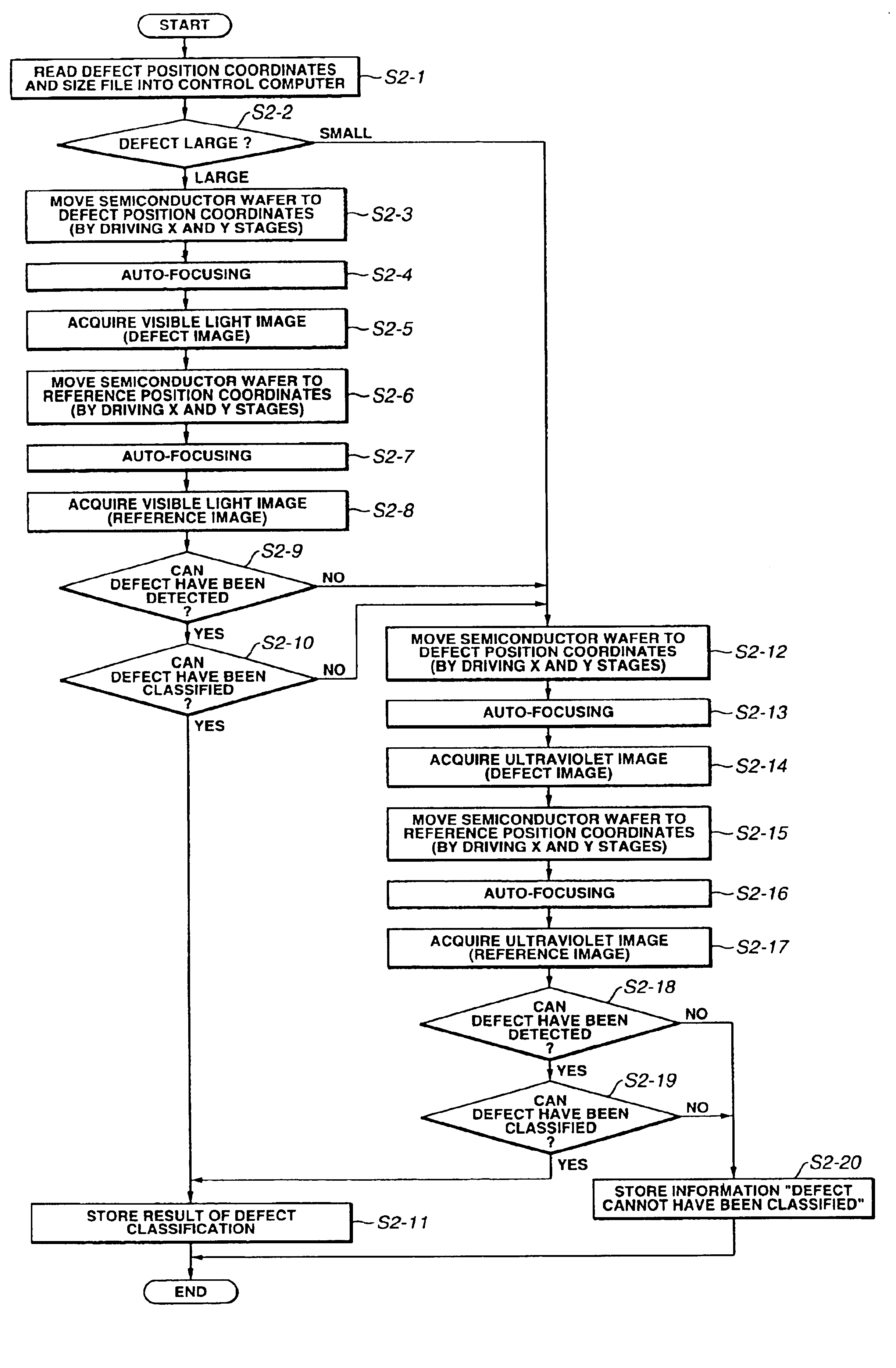
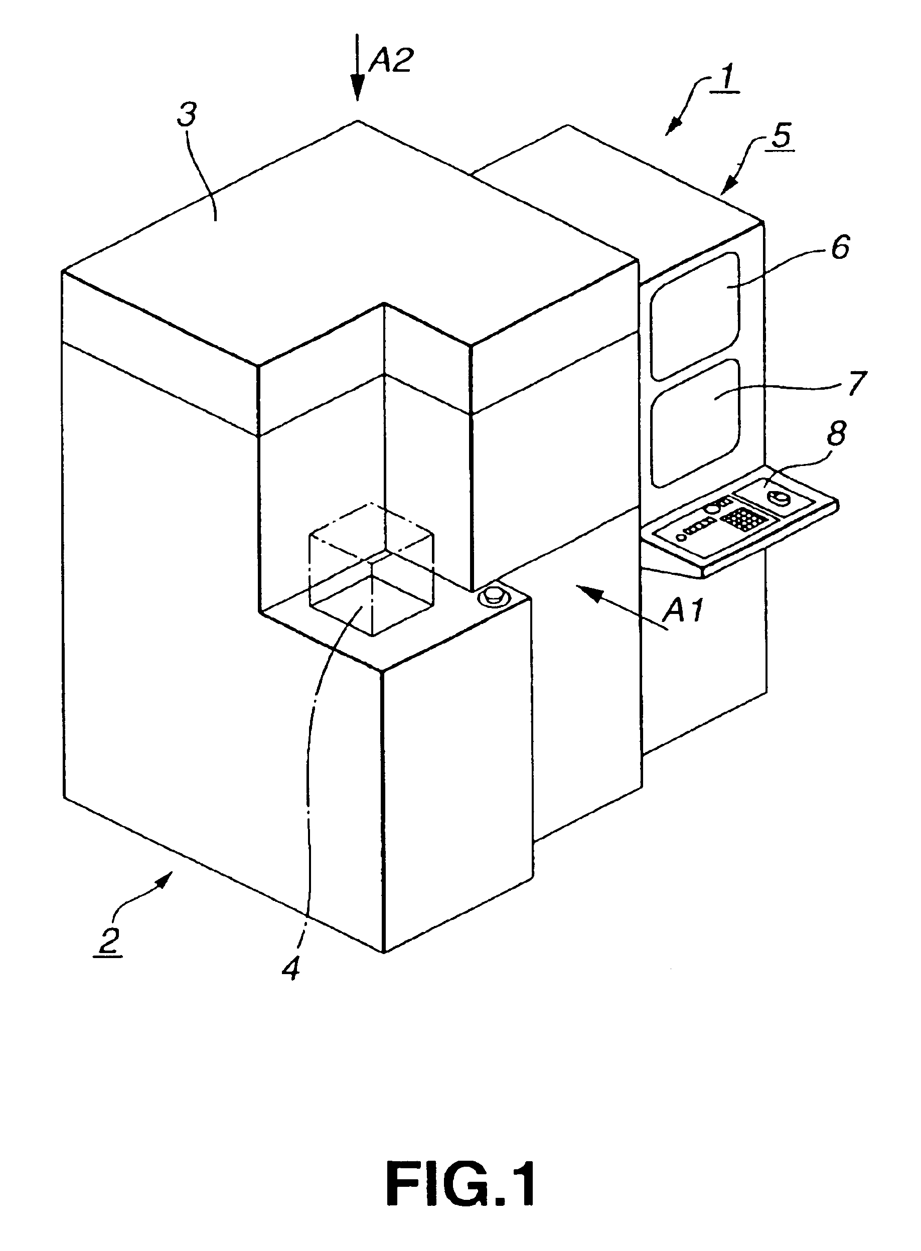
[0030]Referring now to FIG. 1, there is given an external view of the inspection equipment according to the present invention. The inspection equipment is generally indicated with a reference 1. This inspection equipment is intended for inspection of a semiconductor wafer having a predetermined device pattern formed thereon. When a defect is found in the semiconductor wafer having the predetermined device pattern formed therein, the inspection equipment is used to examine what the defect is and classify the defect.

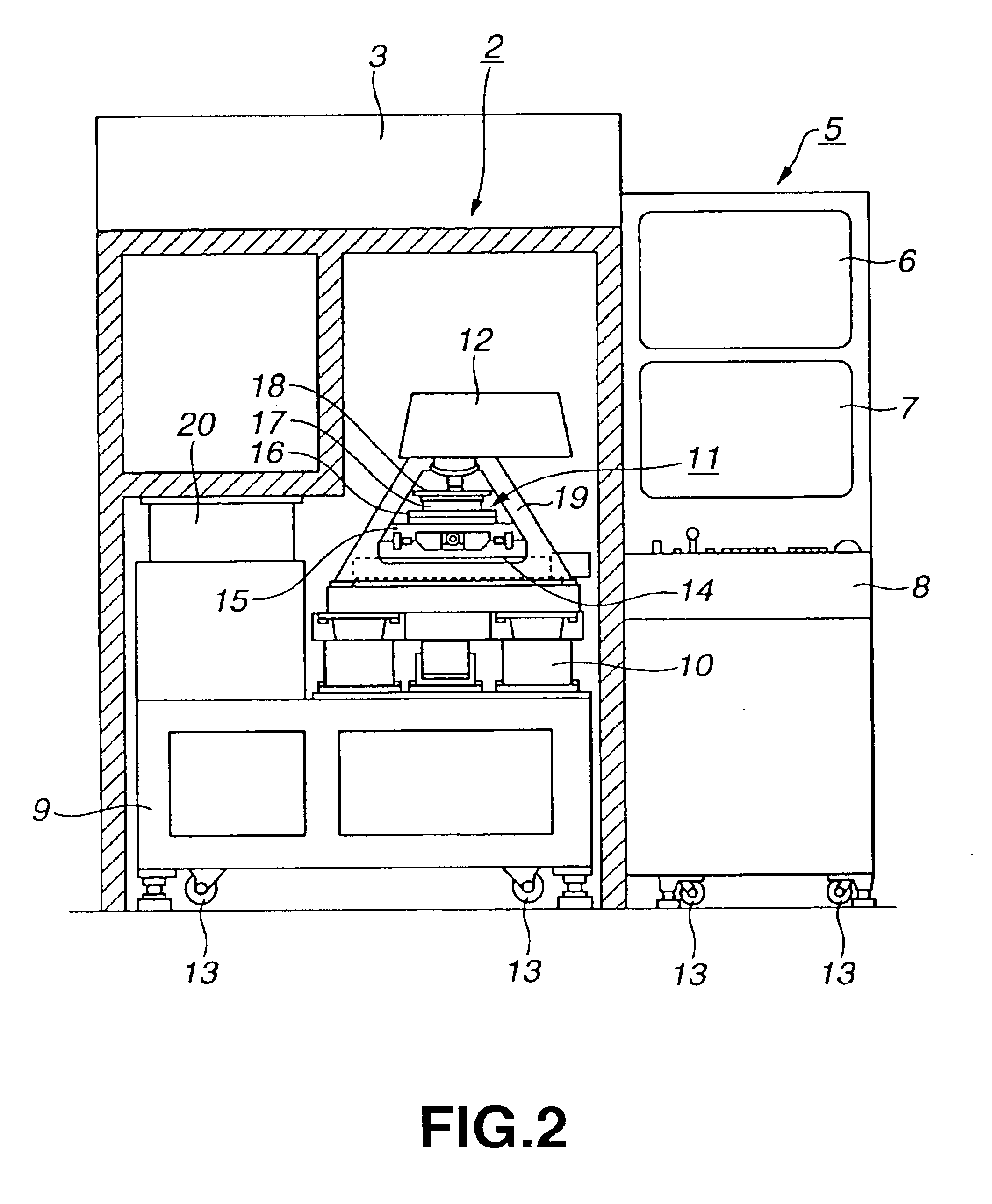
[0031]As shown in FIG. 1, the inspection equipment 1 includes a dedusting clean unit 2 to keep clean the internal environment in the inspection equipment. The clean unit 2 has provided atop thereof a clean air unit 3 to supply clean air from which dust has been removed. With the dust-free clean air supplied from the clean air unit 3, the air cleanliness in the internal environment can be kept at the Class I or so.

[0032]In the clean unit 2 of the inspection equipment 1, a s...


PUM


Abstract

To inspect a finer device pattern formed in a semiconductor wafer, there is provided an inspection equipment including means for supporting a semiconductor wafer as a specimen and moving it to a predetermined position of inspection, means for projecting an ultraviolet light onto the specimen supported on the specimen supporting means, an ultraviolet imaging means for detecting a reflected light or transmitted light from the specimen illuminated by the ultraviolet light projecting means and picking up an image of the specimen, means for processing the image picked up by the ultraviolet imaging means. The image picked up by the imaging means is processed and analyzed by the image processing means to inspect the specimen.

Description

RELATED APPLICATION DATA[0001]The present application claims priority to Japanese Application No. P11-164448 filed Jun. 10, 1999, which application is incorporated herein by reference to the extent permitted by law.BACKGROUND OF THE INVENTION[0002]1. Field of the Invention[0003]The present invention relates to an inspection equipment used to inspect a semiconductor wafer having a predetermined device pattern formed therein, and the like.[0004]2. Description of the Related Art[0005]A semiconductor device is produced with a fine device pattern formed on a semiconductor wafer. In forming such a device pattern, dust or scratch on the semiconductor wafer surface will cause a defect. The semiconductor incurring such a defect is rejected as an unacceptable device, which will lower the yield at the semiconductor device production line.[0006]Accordingly, to stabilize the yield of the production line at a high level, it is necessary to early find a defect caused by dust or scratch, locate the...

Claims


Application Information

Patent Timeline
IPC IPC(8): G01N21/88G01N21/956G01B11/24G01B11/245G01B11/30G01M11/00G01N21/94H01L21/66
CPCG01N21/956H01L22/00
Inventor EGUCHI, NAOYA
Owner SONY CORP
Why Eureka
Try Eureka