Pixel structure
a technology of liquid crystal display and pixel structure, which is applied in the direction of semiconductor devices, optics, instruments, etc., can solve the problems of complex driving circuit and fabrication process, possible failure, and failure of the entire pixel structure, and achieve the effect of improving problems
- Summary
- Abstract
- Description
- Claims
- Application Information
AI Technical Summary
Benefits of technology
Problems solved by technology
Method used
Image
Examples
first embodiment
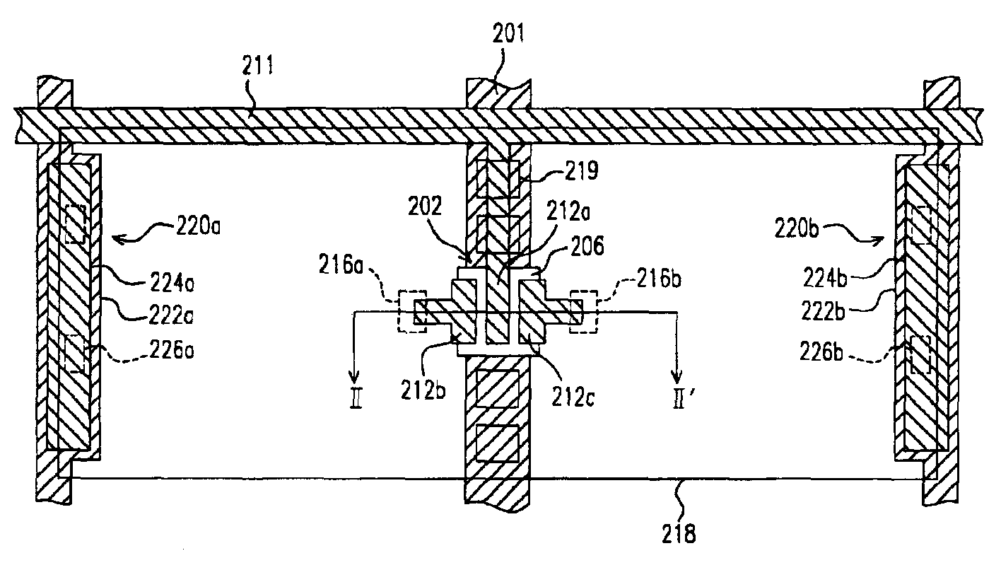
[0026]FIG. 3 is the top view of a pixel structure according to this invention and FIG. 4 is a sectional view through line II-II″ as shown in FIG. 3. As shown in FIGS. 3 and 4, a substrate 200 such as a transparent glass substrate or a transparent plastic substrate is provided. A scan line 201 and a gate 202 are formed over the substrate 200 such that the scan line 201 and the gate 202 are electrically connected.
[0027]Thereafter, a gate dielectric layer 204 is formed over the substrate 200 globally covering the scan line 201 and the gate 202. The gate dielectric layer 204 is fabricated using a dielectric material including silicon nitride or silicon oxide, for example.
[0028]A channel layer 206 is formed over the gate dielectric layer 204 above the gate 202. The channel layer 206 is fabricated using a material such as amorphous silicon. Next, a source 212a and two drains 212b, 212c are formed over the channel layer 206. In the meantime, a data line 211 having connection with the sourc...
second embodiment
[0036]FIG. 5 is the top view of a pixel structure according to this invention and FIG. 7 is a sectional view through line III-III″ of FIG. 5. As shown in FIGS. 5 and 7, a substrate 300 such as a transparent glass substrate or a transparent plastic substrate is provided. A scan line 301 and a gate 302 are formed over the substrate 300 such that the scan line 301 and the gate 302 are electrically connected.
[0037]Thereafter, a gate dielectric layer 304 is formed over the substrate 300 globally covering the scan line 301 and the gate 302. The gate dielectric layer 304 is fabricated using a dielectric material including silicon nitride or silicon oxide, for example.
[0038]A channel layer 306 is formed over the gate dielectric layer 304 above the gate 302. The channel layer 306 is fabricated using a material such as amorphous silicon.
[0039]Next, a source 312a and two drains 312b, 312c are formed over the channel layer 306. At the same time, a data line 311 having connection with the source...
PUM
| Property | Measurement | Unit |
|---|---|---|
| transparent | aaaaa | aaaaa |
| parasitic capacitance | aaaaa | aaaaa |
| metallic | aaaaa | aaaaa |
Abstract
Description
Claims
Application Information


