Clock skew verification methodology for grid-based design

a clock skew and verification methodology technology, applied in the direction of instruments, computing, electric digital data processing, etc., can solve the problems of increasing the size and power consumption of an ic, reducing the performance, and consuming more die area and power

Inactive Publication Date: 2005-09-06
ORACLE INT CORP
View PDF31 Cites 18 Cited by
  • Summary
  • Abstract
  • Description
  • Claims
  • Application Information

AI Technical Summary

Problems solved by technology

Depending on the circumstances and relative to the two elements exchanging data, clock skew may either make the clock signal too early or too late.
Excessive clock skew can decrease the performance and increase the size and power consumption of an IC.
This results in more die area and power being consumed.
This increases production costs and design times.
The cost to analyze the insertion delay for a given path increases in general more than linearly with the size of the problem.
Analyzing the insertion delay of a large path is generally much more computationally expensive than dividing the large path into several smaller paths and analyzing each of these smaller paths separately.
The analysis of all of the insertion delays in a microprocessor design is typically an extremely large computational task, which exceeds any available computational resources as a single analysis task.
Therefore, it is not generally possible to analyze each clocked element separately.
Since conventionally the computation task cannot be separated easily into sub-tasks as with the tree-based clock net above, analyzing the clock insertion delay in a grid-based design is much more difficult than in a tree-based design and requires potentially a much higher computatio

Method used


Image

  • Clock skew verification methodology for grid-based design
  • Clock skew verification methodology for grid-based design
  • Clock skew verification methodology for grid-based design

Examples


Embodiment Construction

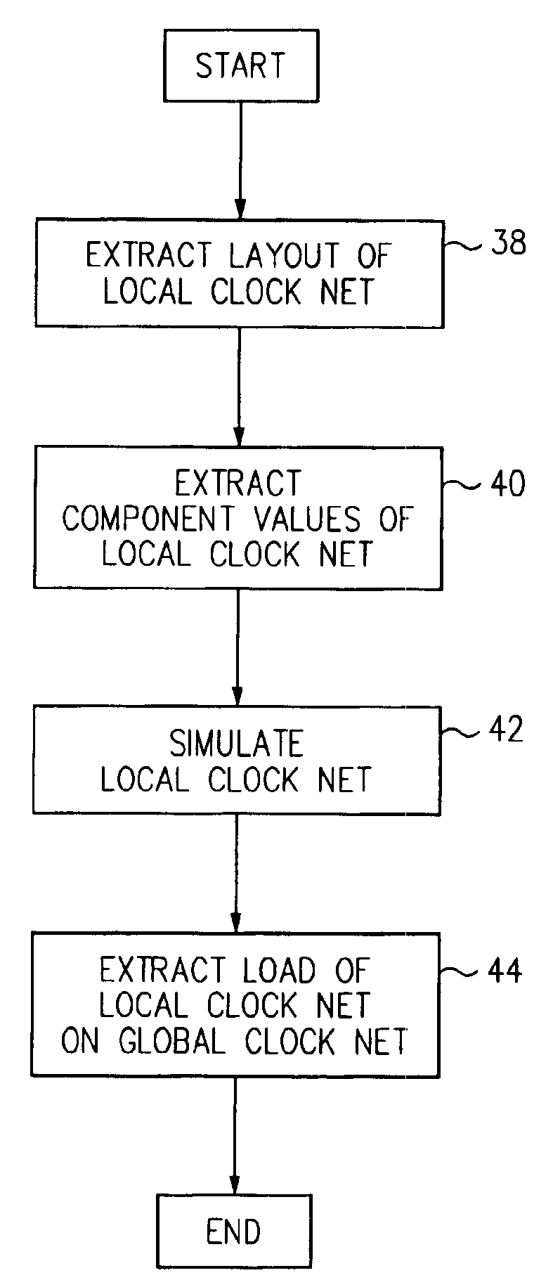
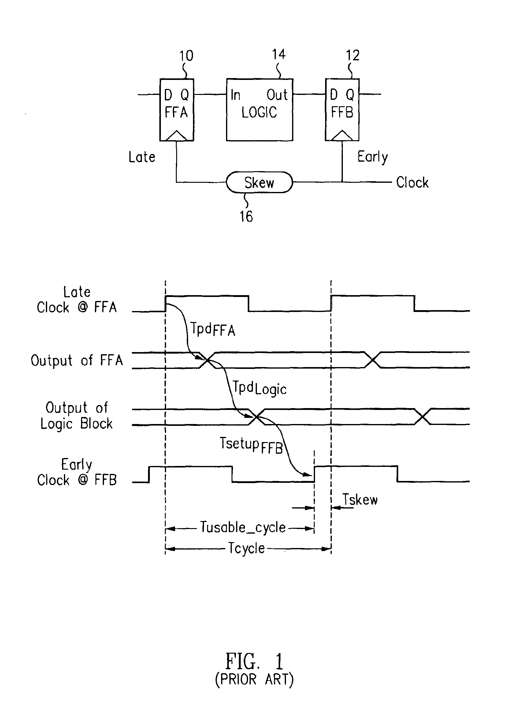
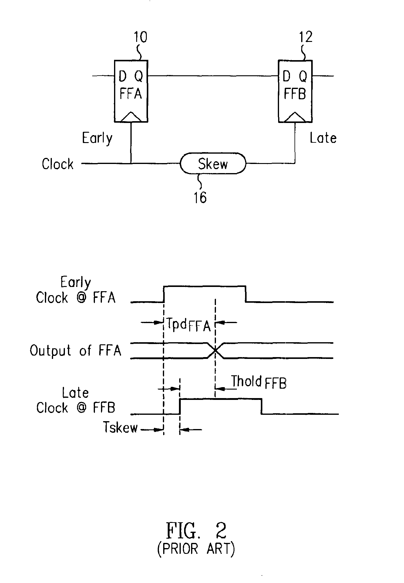
[0024]Embodiments of the present invention are described herein in the context of a clock skew verification methodology for a grid-based clock distribution design. Those of ordinary skill in the art will realize that the following detailed description of the present invention is illustrative only and is not intended to be in any way limiting. Other embodiments of the present invention will readily suggest themselves to such skilled persons having the benefit of this disclosure. Reference will now be made in detail to implementations of the present invention as illustrated in the accompanying drawings. The same reference indicators will be used throughout the drawings and the following detailed description to refer to the same or like parts.

[0025]In the interest of clarity, not all of the routine features of the implementations described herein are shown and described. It will, of course, be appreciated that in the development of any such actual implementation, numerous implementatio...


PUM


Abstract

A method and apparatus for determining clock insertion delays for a microprocessor design having a grid-based clock distribution. The method includes partitioning the complete clock net into a global clock net and a plurality of local clock nets, simulating a load for each of the local clock nets, simulating the global clock net, and combining the simulations to form the complete clock net. The method may further include evaluating the combination to determine whether the results converge and storing the simulation results in a Clock Data Model. When the results do not converge, the method re-simulates at least one of the local clock nets and re-simulates the global clock net. The Clock Data Model collects, manages, retrieves, and queries all of the simulation information. The method may further analyze the complete clock net to predict the clock skew for a given data transfer path for potential redesign.

Description

CROSS-REFERENCE TO RELATED APPLICATIONS[0001]This application is related to U.S. patent application Ser. No. 09 / 982,459, entitled “Unified Database System to Store, Combine, and Manipulate Clock Related Data for Grid-Based Clock Distribution Design,” in the name of Ralf M. Schmitt and Manjunath D. Haritsa, now published as 2003 / 0074643 A1, and U.S. patent application Ser. No. 09 / 982,458, entitled “Simulation by Parts method for Grid-Based Clock Distribution Design,” in the name of Manjunath D. Haritsa and Ralf M. Schmitt, now published as 2003 / 0074175A1, both filed on an even date herewith and commonly assigned wherewith.FIELD OF THE INVENTION[0002]The present invention relates generally to a method for determining clock circuitry parameters in an integrated circuit design. More specifically, the present invention relates to employing clock net data to determine clock insertion delays for a microprocessor design having grid-based clock distribution.BACKGROUND OF THE INVENTION[0003]C...

Claims


Application Information

Patent Timeline
IPC IPC(8): G06F17/50
CPCG06F17/5022G06F2217/62G06F30/33G06F30/396G06F30/3308
Inventor HARITSA, MANJUNATH D.ANKOLA, MANISHKUMAR B.SCHMITT, RALFSHARMA, ANUPHOEROLD, STEPHANMURATA, DAVID MINORU
Owner ORACLE INT CORP
Why Eureka
Try Eureka