Magnetic storage apparatus and manufacturing method thereof

a magnetic storage device and manufacturing method technology, applied in solid-state devices, nanoinformatics, instruments, etc., can solve the problems of difficult microprocessing of ferroelectric capacitors, slow write speed, and difficult integration to a large degree, so as to avoid waste in terms of occupied area and effectively layout semiconductor regions

Inactive Publication Date: 2005-09-13
SONY CORP
View PDF8 Cites 11 Cited by
  • Summary
  • Abstract
  • Description
  • Claims
  • Application Information

AI Technical Summary

Benefits of technology

[0015]Accordingly, this makes it possible to isolate the semiconductor regions in which the read transistors are to be made, using the element isolation regions in an effective manner, while avoiding waste in terms of occupied area. It is also made possible to reduce contact holes for connecting the diffusion layers of the read transistors and the bit lines without causing short-circuiting of the individual semiconductor regions, and this makes it possible to avoid short-circuiting between the semiconductor regions even if the storage cells are further down-sized as compared with the contact holes.
[0018]Moreover, one end portion of each of a plurality of semiconductor regions which compose a second semiconductor region array adjacent to a first semiconductor region array comprising a plurality of the semiconductor regions arranged in the extending direction of the write word line can be arranged one by one between the individual semiconductor regions in the first semiconductor region array on the second semiconductor region array side. This makes it possible to effectively layout the semiconductor regions in which the read transistors are to be made while avoiding waste in terms of occupied area.
[0019]This also solves the problem of cross-talk because distance between the individual magnetic storage elements and distance between the individual write word lines can be ensured to a sufficient degree.

Problems solved by technology

The flash memory, however, suffers from a problem that it is hard to be integrated to a large degree due to its complicated structure, and that it has only a write speed as slow as having an order of microsecond.
Difficulty in microprocessing of the ferroelectric capacitor is also pointed out as a problem.
Higher integration and consequently thinned wirings, however, inevitably reduce critical current value allowable by a write line to thereby weaken an obtainable magnetic field, and this unwillingly decreases coercive force of a recordable region.
This means decrease in reliability of the information recording element.
Moreover, a magnetic field cannot be condensed unlike light or electron beam, and this may possibly be a major cause for cross-talk in a case of a highly-integrated element.

Method used


Image

  • Magnetic storage apparatus and manufacturing method thereof
  • Magnetic storage apparatus and manufacturing method thereof
  • Magnetic storage apparatus and manufacturing method thereof

Examples


Embodiment Construction

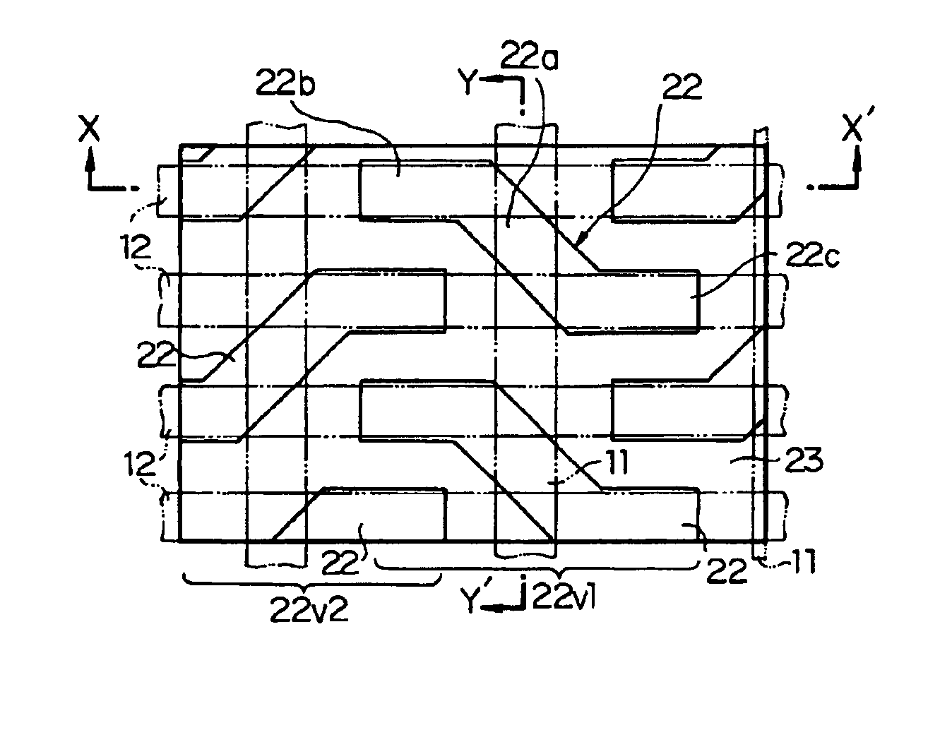
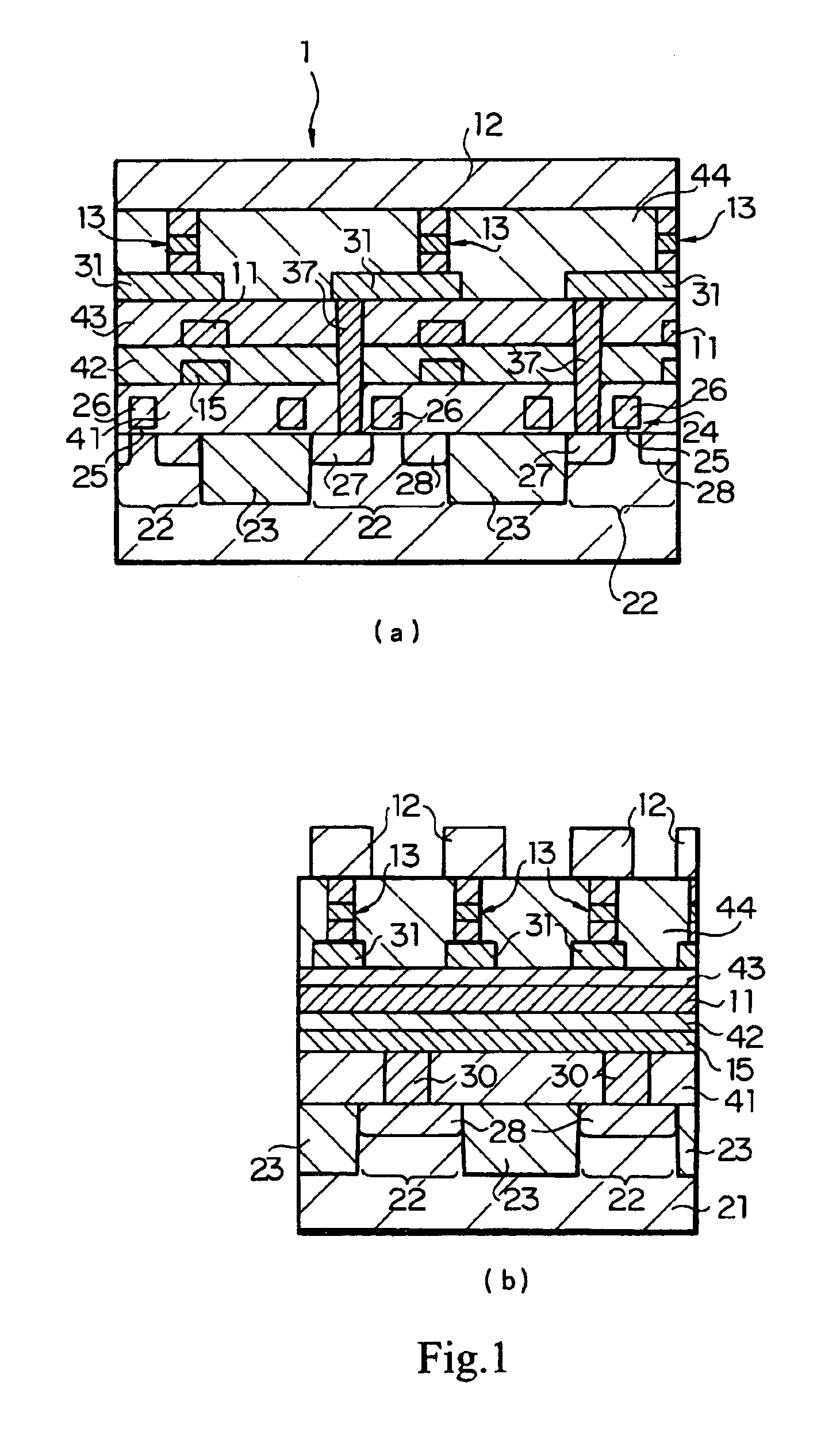
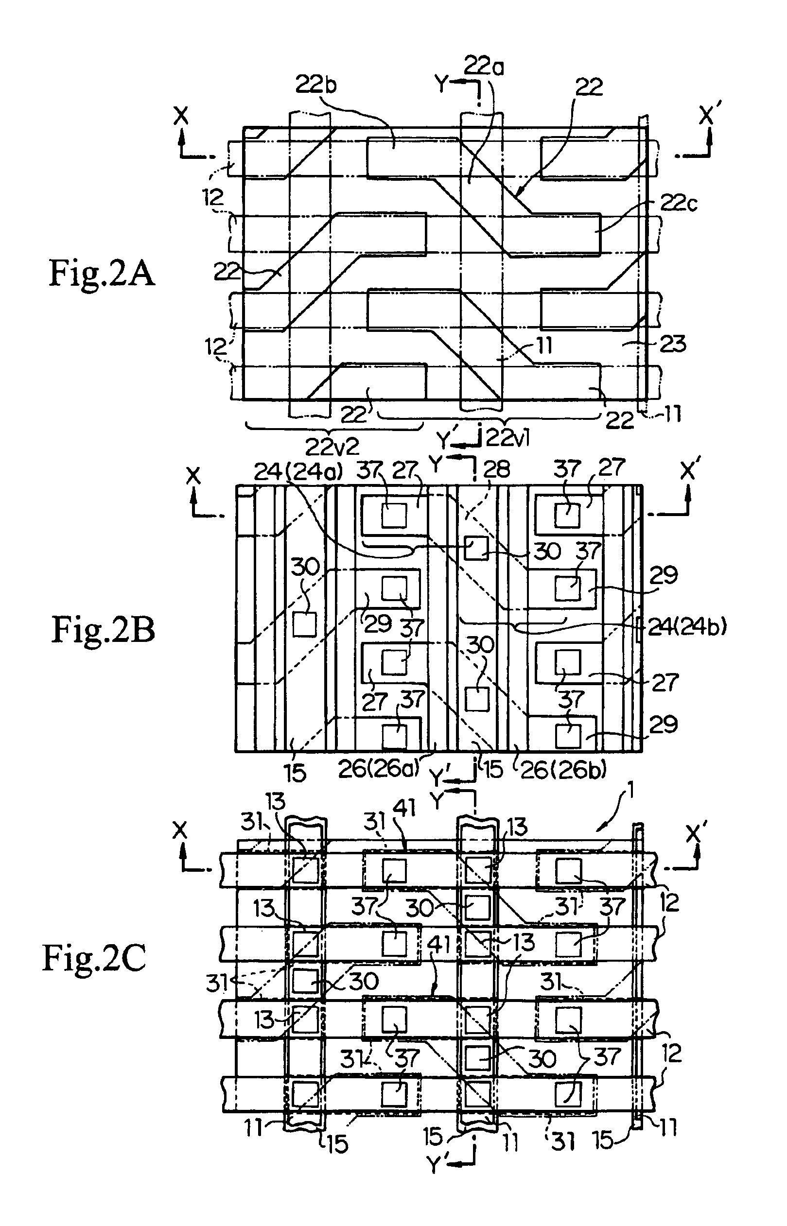
[0031]First, a general MRAM (Magnetic Random Access Memory) will be explained referring to FIG. 3 which is a schematic structural perspective view showing an essential portion thereof in a simplified manner. In FIG. 3, illustration of the read-out circuit portion is omitted for simplicity.

[0032]It includes nine memory cells, as can be seen in FIG. 3, where write word lines 11 (111, 112, 113) and bit lines 12 (121, 122, 123) are disposed so as to cross with each other. At intersectional regions of the write word lines 11 and the bit lines 12, magnetoresistance effect (TMR) elements 13 (131 to 139) are disposed as magnetic storage elements. Write operation to the TMR elements 13 are accomplished by allowing electric current to flow in the bit lines 12 and the write word lines 11, and changing the direction of magnetization of the storage layer 304 (see FIG. 6 for detail) of the TMR elements 13, formed at the intersections between the bit lines 12 and the write word lines 11, into para...


PUM


Abstract

Problems in reliability and cross-talk of MRAM, which are intrinsically ascribable to the structure thereof, are solved at the same time. In a magnetic storage device (1) having write word lines (11) and bit lines (12) formed so as to cross while keeping a predetermined space therebetween, and provided with a TMR element (13) configured so as to sandwich a tunnel insulating layer (303) with a magnetization fixed layer (302) and a storage layer (304) comprising a ferromagnetic layer, in each of thus-formed intersectional region, and there is provided a semiconductor region (22) in which two read transistors (24, 24), which serve as read transistors, are formed, and which comprises a first region (22a) obliquely crosses a projected region of the write word line (11); a second region (22b) formed in parallel with the bit line (12) so as to be continued from one end of the first region; and a third region (22c) formed in parallel with the bit line (12) and so as to be continued from the other end of the first region (22a).

Description

BACKGROUND OF THE INVENTION[0001]The present invention relates to a magnetic storage device and a method of fabricating the same, and more specifically to a non-volatile magnetic storage device configured so as to store information in response to changes in resistance value depending on parallel or antiparallel alignment of spin of a ferromagnetic material composing a tunnel magnetoresistance element, and a method of fabricating the same.[0002]With a dramatic popularization of information communication instruments in particular of mobile terminals, there are increasing demands for further advanced performances of elements such as memory elements and logic elements, with regard to higher degree of integration, higher speed, and lower power consumption. In particular, non-volatile memory is considered as an indispensable element in the ubiquitous era.[0003]For example, non-volatile memory can protect important personal information even when exhaustion or any troubles occurred in power...

Claims


Application Information

Patent Timeline
Patent Type & Authority Patents(United States)
IPC IPC(8): G11C11/15H01L29/66H01L21/70G11C11/14H01L21/00H01L29/76G11C11/02H01L29/00H01L21/8234H01L27/105H01L31/101H01L31/113H01L43/08G11C19/08H01L21/8246H01L27/22
CPCB82Y10/00H01L27/228H10B61/22G11C11/15
Inventor YOSHIHARA, IKUOMOTOYOSHI, MAKOTO
Owner SONY CORP
Why Eureka
Try Eureka