Semiconductor integrated circuit device

a technology of integrated circuit devices and semiconductors, which is applied in the direction of transistors, solid-state devices, instruments, etc., can solve the problems of increasing the increasing the difficulty of cutting polyfuses with existing laser equipment, so as to reduce the size and cost of semiconductor integrated circuit devices, reduce the number of connectors, and simplify manufacturing facilities

Inactive Publication Date: 2005-09-13
ROHM CO LTD
View PDF2 Cites 4 Cited by
  • Summary
  • Abstract
  • Description
  • Claims
  • Application Information

AI Technical Summary

Benefits of technology

[0014]According to the present invention, a semiconductor integrated circuit device is provided with a first semiconductor chip having a nonvolatile memory for storing redundancy information, and a second semiconductor chip having a conversion circuit for converting the redundancy information output in the form of serial data from the nonvolatile memory into parallel data and a redundancy circuit of which the output state is definitely set by receiving the parallel data output from the conversion circuit. This makes it possible to definitely set the output state of the redundancy circuit without a laser beam. In this way, it is possible to realize a semiconductor integrated circuit device that permits the output state of a redundancy circuit to be definitely set easily even with an increased number of conductor layers. Moreover, there is no need to use laser equipment any longer. This helps simplify the manufacturing facilities.
[0015]Moreover, according to the present invention, data transfer from the nonvolatile memory to the conversion circuit is achieved in the form of serial data. This helps reduce the number of connectors (for example, bumps) by way of which the nonvolatile memory and the conversion circuit are connected together. This helps reduce the size and cost of the semiconductor integrated circuit device as compared with in a case where data transfer from the nonvolatile memory to the conversion circuit is achieved in the form of parallel data.

Problems solved by technology

5), and thus has been making it increasingly difficult to cut the polyfuses 16 with a laser beam unless the windows are made accordingly large.
As the number of conductor layers further increases in future, the windows need to be made increasingly small according to design rules, until eventually it becomes impossible to cut the polyfuses with existing laser equipment.
However, as compared with polyfuses, metal fuses are liable to cutting failure resulting from refusing or the like after cutting with a laser beam.

Method used


Image

  • Semiconductor integrated circuit device
  • Semiconductor integrated circuit device
  • Semiconductor integrated circuit device

Examples


Embodiment Construction

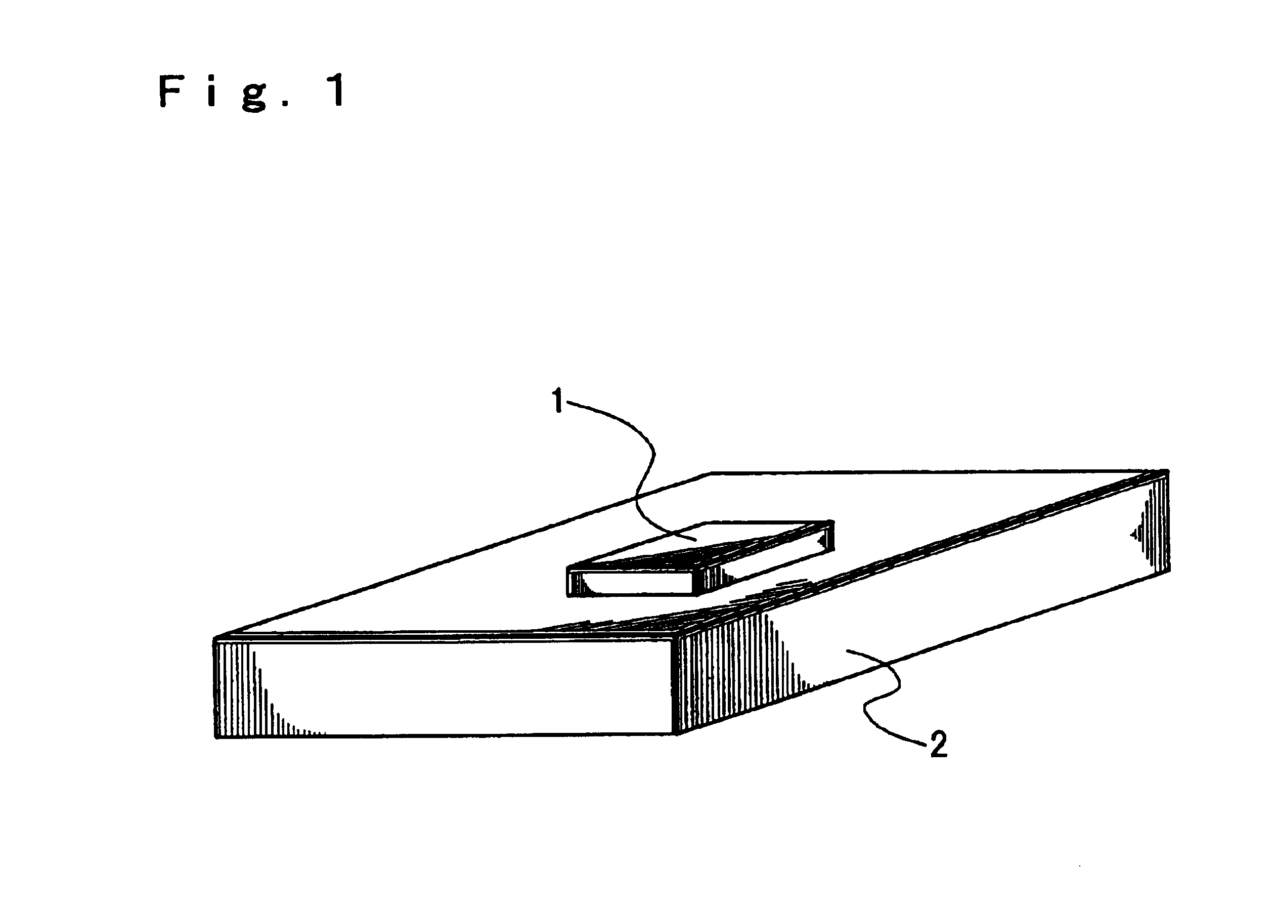
[0022]FIG. 1 is an external view of a semiconductor integrated circuit device according to the present invention. A first semiconductor chip 1 and a second semiconductor chip 2 are connected together by way of bumps (not illustrated). The second semiconductor chip 2 has a memory IC, a memory circuit, and a CPU circuit previously incorporated in it to form a semiconductor integrated circuit (not illustrated) generally called an embedded IC.

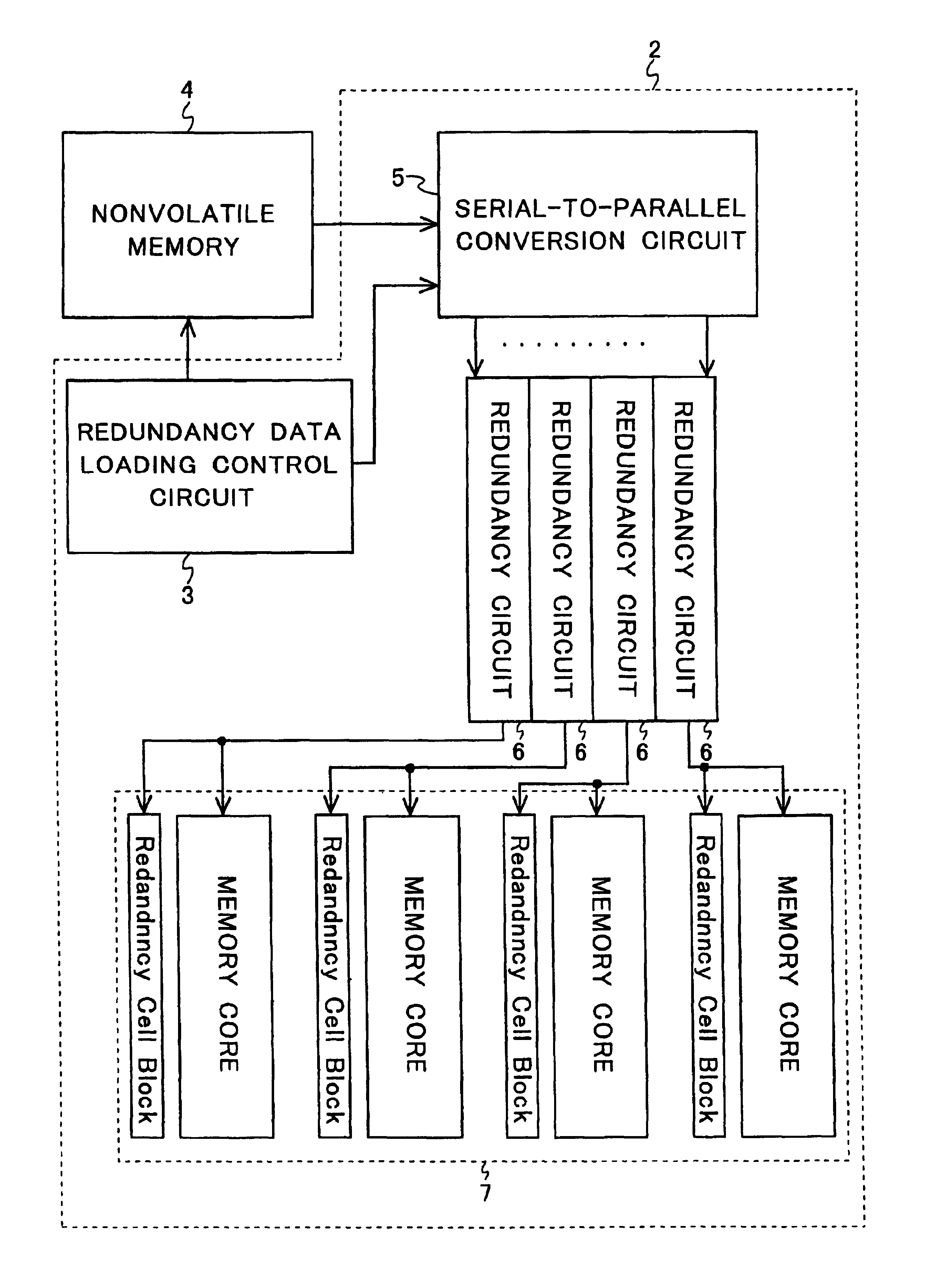
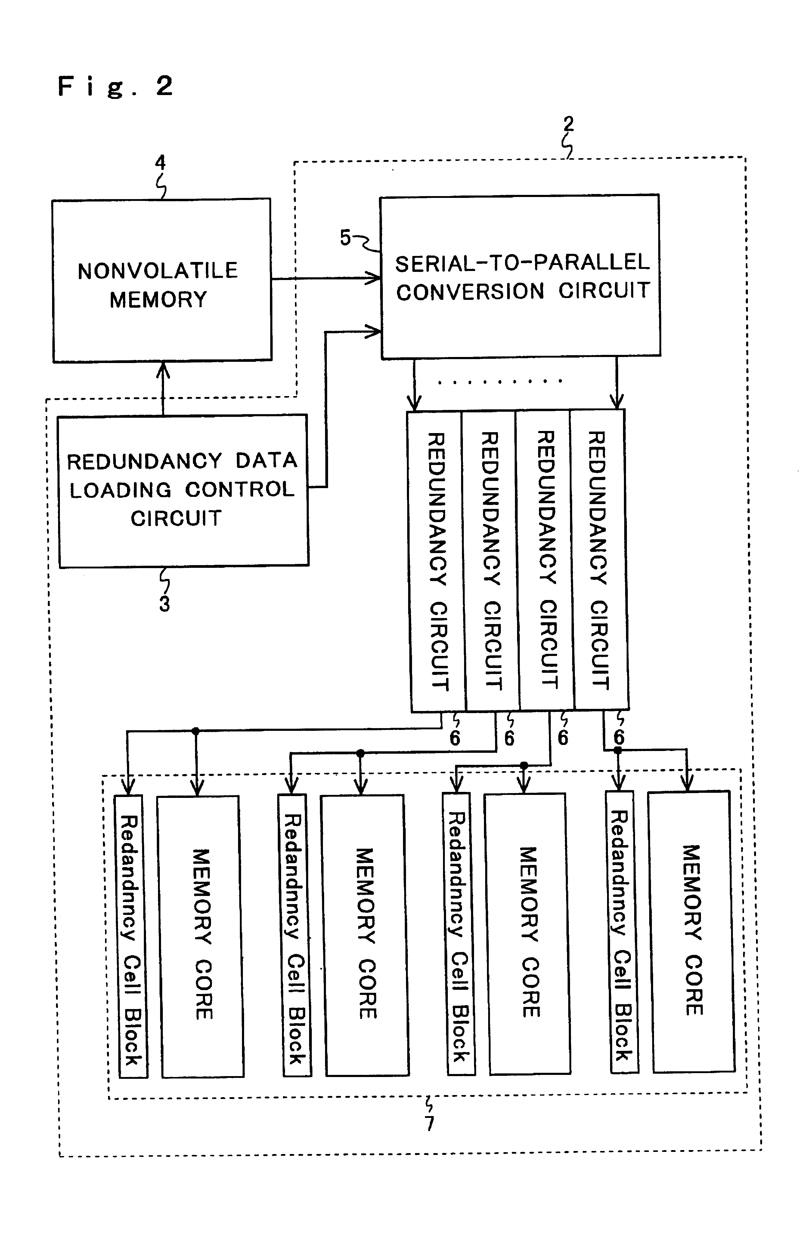
[0023]FIG. 2 is a circuit block diagram of a principal portion of the semiconductor integrated circuit device according to the invention. The semiconductor integrated circuit device according to the invention has a redundancy data loading control circuit 3, a nonvolatile memory 4, a serial-to-parallel conversion circuit 5, a plurality of redundancy circuits 6, and a plurality of functional circuits 7, such as memories, having circuits that are individually selected or unselected by the redundancy circuits 6. The nonvolatile memory 4, such as a flas...


PUM


Abstract

A conventional semiconductor integrated circuit device suffers from the increasing difficulty in definitely setting the output state of a redundancy circuit as the number of conductor layers increases. To overcome this inconvenience, according to the present invention, a semiconductor integrated circuit device has a first semiconductor chip having a nonvolatile memory for storing redundancy information, and has a second semiconductor chip having a conversion circuit for converting the redundancy information output in the form of serial data from the nonvolatile memory into parallel data and a redundancy circuit of which the output state is definitely set by receiving the parallel data output from the conversion circuit.

Description

[0001]This application is based on Japanese Patent Application No. 2002-349987 filed on Dec. 2, 2002, the contents of which are hereby incorporated by reference.BACKGROUND OF THE INVENTION[0002]1. Field of the Invention[0003]The present invention relates to a semiconductor integrated circuit device, and more particularly to a semiconductor integrated circuit device provided with a redundancy circuit.[0004]2. Description of the Prior Art[0005]A semiconductor integrated circuit such as a memory usually incorporates a redundancy circuit by the use of which an effective circuit block is selected. This helps increase the yield of the product. FIG. 4 shows an example of the configuration of a conventional redundancy circuit. The redundancy circuit shown in FIG. 4 is composed of N+1 address program circuits AP0 to APN and an AND circuit 14 that outputs, as a signal REDEN, the AND of the outputs of the individual address program circuits AP0 to APN. Each address program circuit is composed ...

Claims


Application Information

Patent Timeline
Patent Type & Authority Patents(United States)
IPC IPC(8): G11C7/00H01L29/66H01L21/70H01L25/065H01L27/115G11C29/00H01L21/822H01L21/82H01L21/8247H01L29/788H01L27/10H01L27/00H01L25/18H01L29/792H01L25/07H01L27/04G11C29/04
CPCG11C29/802H01L2924/0002H01L2924/00
Inventor SATO, KAZUO
Owner ROHM CO LTD
Why Eureka
Try Eureka