Electronic circuit device and method for manufacturing same

a technology of electronic circuit device and manufacturing method, which is applied in the direction of final product manufacturing, solid-state device, synthetic resin layered product, etc., can solve the problems of difficult mounting of electronic components, device damage, and difficult to change the shape of anisotropic conductive film in the radiation-hardened region, so as to simplify the manufacturing steps of electronic circuit device and simplify the manufacturing steps. , the effect of simple steps

Inactive Publication Date: 2009-05-28
PANASONIC CORP
View PDF28 Cites 16 Cited by
  • Summary
  • Abstract
  • Description
  • Claims
  • Application Information

AI Technical Summary

Benefits of technology

[0016]According to this method, it is possible to manufacture an electronic circuit device by coupling the electronic components, for example, a combination of a semiconductor element and a passive component, or semiconductor elements having different thicknesses, and the like, by the same mounting method using the same anisotropic conductive resin layer. Consequently, the manufacturing steps can be simplified.
[0017]According to the electronic circuit device of the present invention having the above-mentioned configuration and manufacturing method, electronic components such as passive components and semiconductor elements for manufacturing various kinds of electronic circuit can be mounted by simple steps. Therefore, the manufacturing steps of the electronic circuit device can be simplified and manufacturing facility can be simplified. Therefore, various electronic circuit devices can be produced at a low cost, and a flexible manufacturing process can be realized

Problems solved by technology

Furthermore, it is difficult to change the shape of the anisotropic conductive film in the region hardened by radiation.
However, such pressing power is applied to these devices, the devices may be damaged.
However, in this method, it is difficult to mount electronic components in which the intervals between electrode terminals and connection terminals vary.
In this method, the production steps become complicated.

Method used


Image

  • Electronic circuit device and method for manufacturing same
  • Electronic circuit device and method for manufacturing same
  • Electronic circuit device and method for manufacturing same

Examples


first exemplary embodiment

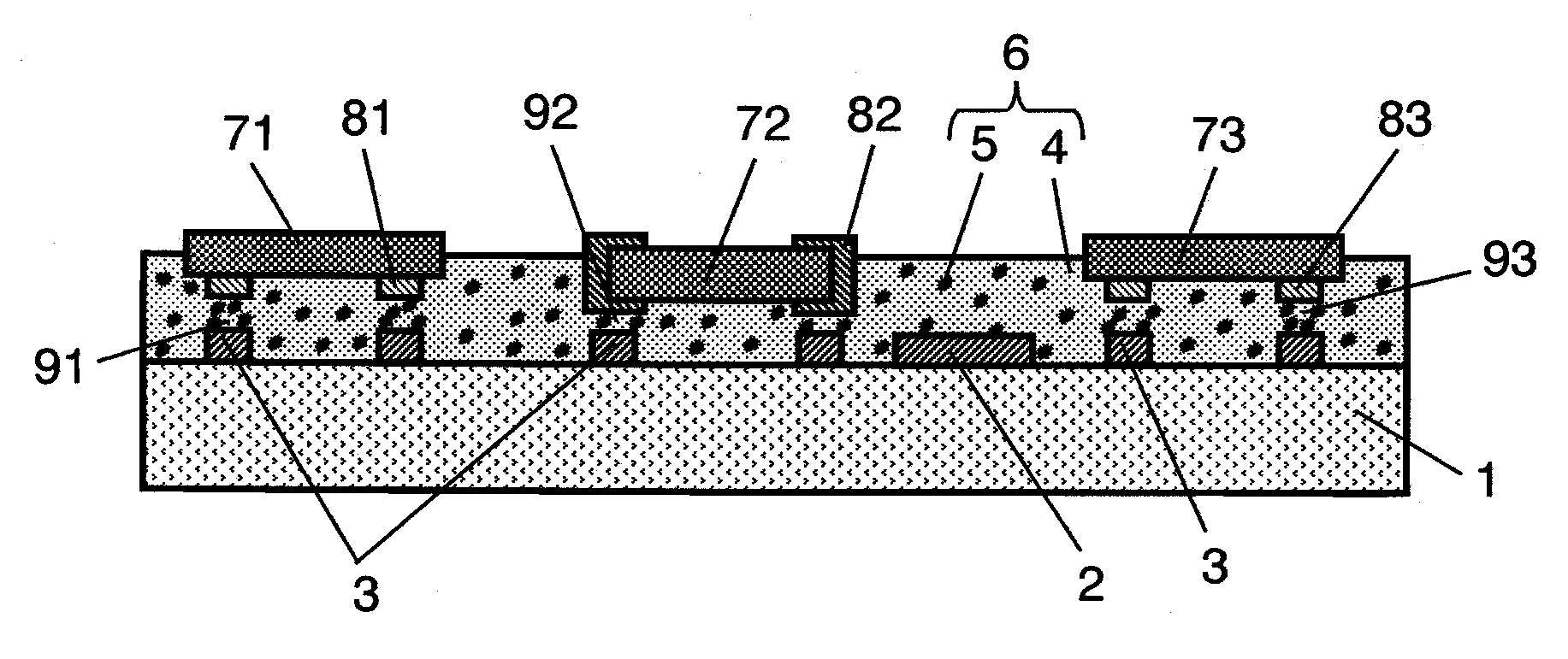
[0072]FIGS. 1A and 1B are sectional views showing configurations of two kinds of electronic circuit devices in accordance with a first exemplary embodiment of the present invention. The difference in the configurations of the electronic circuit devices between FIG. 1A and FIG. 1B is as follows. That is to say, the thicknesses of electronic components, first electronic component 71, second electronic component 72 and third electronic component 73 are different from each other. In the configuration of FIG. 1A, these electronic components are disposed so that their rear surfaces are in the same plane. In FIG. 1B, the components are disposed so that intervals 91, 92, and 93 between connection terminal 3 and electrode terminals 81, 82, and 83 become the same.

[0073]As shown in FIG. 1A, the electronic circuit device in accordance with this exemplary embodiment includes circuit board 1 having conductor wiring 2 and connection terminal 3 on one surface thereof; anisotropic conductive resin l...

second exemplary embodiment

[0089]FIGS. 3A to 3C are sectional views to illustrate a method for manufacturing an electronic circuit device in accordance with a second exemplary embodiment of the present invention.

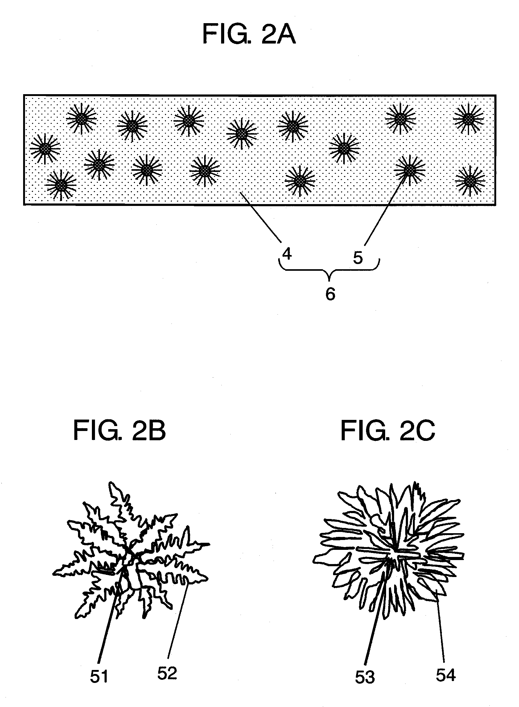
[0090]Firstly, as shown in FIG. 3A, on the main surface of circuit board 1 including conductor wiring 2 and connection terminal 3 thereon, anisotropic conductive resin layer 6 is formed. The steps shown in FIGS. 3A to 3C illustrate an example using anisotropic conductive resin layer 6 in which conductive particles 5 having the shape shown in FIG. 2C are dispersed in resin binder 4 including a photocurable insulating resin and a thermosetting insulating resin and having a surface tackiness. Anisotropic conductive resin layer 6 may be formed by attaching a sheet-shaped anisotropic conductive resin or by printing a paste-state anisotropic conductive resin.

[0091]Next, as shown in FIG. 3B, electrode terminals 81 on first electronic component 71 are positioned to connection terminals 3 on circuit board 1, a...

third exemplary embodiment

[0095]FIGS. 4A to 4D are sectional views to illustrate a method for manufacturing an electronic circuit device in accordance with a third exemplary embodiment of the present invention.

[0096]Firstly, as shown in FIG. 4A, on the main surface of circuit board 1 including conductor wiring (not shown) and connection terminal 3 thereon, anisotropic conductive resin layer 6 is formed. Anisotropic conductive resin layer 6 may be formed by attaching a sheet-shaped anisotropic conductive resin or by printing a paste-state anisotropic conductive resin. FIGS. 4A to 4D do not show conductor wiring formed on the surface of circuit board 1, however, similar to the circuit board shown in FIGS. 1A and 1B and FIGS. 3A to 3C, conductor wiring is formed.

[0097]The steps shown in FIGS. 4A to 4D illustrate an example using anisotropic conductive resin layer 6 in which conductive particles 5 shown in FIG. 2C are dispersed in resin binder 4 including a photocurable insulating resin and a thermosetting insul...


PUM

PropertyMeasurementUnit
thicknessaaaaaaaaaa
temperaturesaaaaaaaaaa
thicknessaaaaaaaaaa

Abstract

Circuit board having conductor wiring and connection terminal; anisotropic conductive resin layer provided on one surface of circuit board; and plurality of electronic components respectively provided with electrode terminals in positions facing the connection terminal are included. The anisotropic conductive resin layer includes at least one kind of conductive particles selected from coiled conductive particles, fiber fluff conductive particles and conductive particles provided with a plurality of conductive protrusions, and resin binder; electrically couples electrode terminals of plurality of electronic components to connection terminals to each other with conductive particles; mechanically fixes electronic components and circuit board to each other; and protects conductor wiring.

Description

TECHNICAL FIELD[0001]The present invention relates to an electronic circuit device in which connection terminals on a circuit board and electrode terminals of electronic components are coupled to each other by using an anisotropic conductive resin including elastic conductive particles in a resin binder.BACKGROUND ART[0002]Conventionally, when a flexible circuit board is coupled to a liquid crystal display panel or when electronic components such as a semiconductor component, resistor, capacitor, or the like, are mounted on a circuit board, an anisotropic conductive adhesive or an anisotropic conductive sheet is used for electrically coupling terminals to each other.[0003]FIG. 8A and FIG. 8B are sectional views showing an example of a conventional anisotropic conductive sheet and a coupling method thereof. FIG. 8A and FIG. 8B show a case in which an electronic component such as a semiconductor chip is coupled to a circuit board. However, the same method is employed in the case in wh...

Claims


Application Information

Patent Timeline
Patent Type & Authority Applications(United States)
IPC IPC(8): H05K1/02H01R9/00
CPCC09J9/02Y10T29/49147H01L24/29H01L24/83H01L24/95H01L2221/68354H01L2224/29499H01L2224/83101H01L2224/83136H01L2224/83192H01L2224/83859H01L2924/01002H01L2924/01027H01L2924/01033H01L2924/01047H01L2924/01078H01L2924/01082H01L2924/0781H01L2924/09701H01L2924/19041H01L2924/19042H01L2924/19043H01L2924/19105H01L2924/3011H01L2924/3025H05K3/284H05K3/323H05K2201/0108H05K2201/0281H05K2201/0373H05K2201/10636H05K2201/10674H05K2203/1476H01L2224/2919H01L2924/01006H01L2924/01019H01L2924/0665H01L21/6835Y10T428/254Y10T428/24372H01L2924/07811H01L2924/00Y02P70/50
Inventor NISHIKAWA, KAZUHIROMIYAKAWA, HIDENORITSUKAHARA, NORIHITOSAKATANI, SHIGEAKI
Owner PANASONIC CORP
Why Eureka
Try Eureka