Scalable design for DDR SDRAM buses

a sdram bus and scalable technology, applied in the field of buses, can solve the problems of processor clock speed, processor clock speed, and constant reach of processor clock speed

Inactive Publication Date: 2005-09-13
ORACLE INT CORP
View PDF13 Cites 16 Cited by
  • Summary
  • Abstract
  • Description
  • Claims
  • Application Information

AI Technical Summary

Problems solved by technology

Furthermore, processor clock speeds continually reach previously unattainable speeds on a regular basis, thereby fueling the public's interest.
However, processor clock speed is but one factor in the speed of the computing system as a whole.
If the processor races far beyond the speeds attainable by the memory subsystem, the processor's excess speed results only in unrealized potential as opposed to actual performance.
Even such an improvement as DDR SDRAM can have only limited impact on overall performance of a computing system, however.
With SDRAM and DDR SDRAM, one performance limitation is the physical length of the bus, and especially the traces of the bus, between the processor(s) and the devices of the memory modules.
Each unit length of the bus creates a “propagation delay.” Longer buses have greater the propagation delays that slow their performance.
High speed buses consequently need to be short.
One of the many problems associated with this phenomenon is it hampers the applicability of the SDRAM technology.
Because the buses must be short, SDRAM is relatively difficult to use in memory intensive computing systems, e.g., servers.
Such systems employ large memory subsystems with many memory modules, which requires long buses that induce large propagation delays.
These solutions raise additional complications, however, such as increased complexity and higher cost.
In other words, the SDRAM technology is not very scalable to large memory subsystems because of the physical limitations of the traces and the bus.

Method used


Image

  • Scalable design for DDR SDRAM buses
  • Scalable design for DDR SDRAM buses
  • Scalable design for DDR SDRAM buses

Examples


Embodiment Construction

[0021]Illustrative embodiments of the invention are described below. In the interest of clarity, not all features of an actual implementation are described in this specification. It will of course be appreciated that in the development of any such actual embodiment, numerous implementation-specific decisions must be made to achieve the developers' specific goals, such as compliance with system-related and business-related constraints, which will vary from one implementation to another. Moreover, it will be appreciated that such a development effort, even if complex and time-consuming, would be a routine undertaking for those of ordinary skill in the art having the benefit of this disclosure.

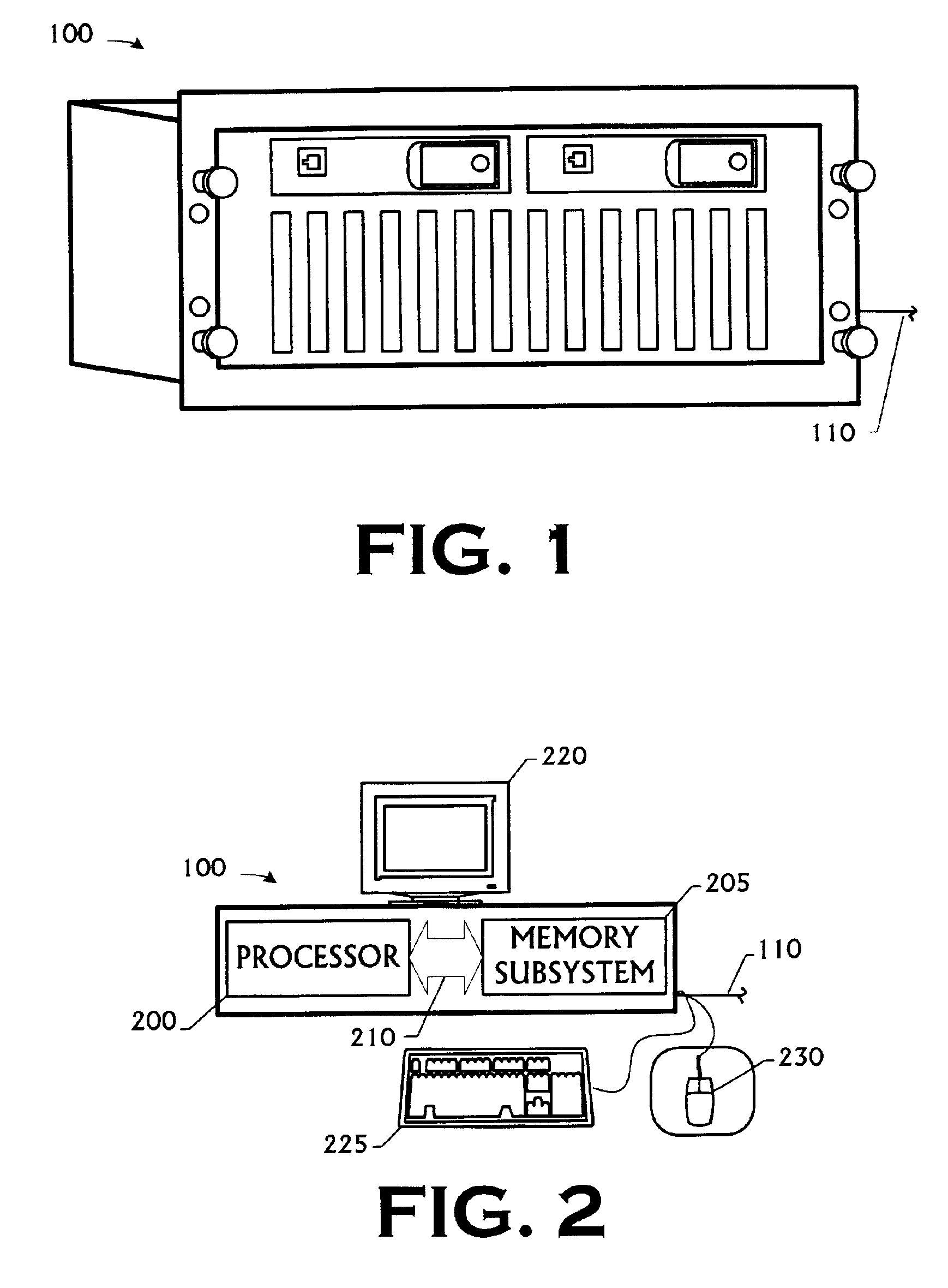
[0022]FIG. 1 depicts in a plan view a computing device 100 manufactured, programmed, and operated in accordance with the present invention. In the illustrated embodiment, the computing device 100 is a Sun Ray™ server employing a UNIX-based operating system (e.g., a Solaris™ OS) commercially avail...


PUM


Abstract

A memory subsystem and a method for use in accessing a memory system are disclosed. The memory subsystem comprising a plurality of SDRAM memory modules and a memory controller. The memory controller is capable of waiting to generate a memory clock signal for each of the SDRAM memory modules until a valid window for a control signal and an address signal; generating the memory clock signals during the valid window, and generating the control and address signals. The method comprises: waiting for a valid window for a control signal and an address signal; generating a memory clock during the valid window; and generating the control signal and the command signal a predetermined period of time after generating the memory clock signal.

Description

BACKGROUND OF THE INVENTION[0001]1. Field of the Invention[0002]The present invention pertains to buses for synchronous dynamic random access memory (“SDRAM”) and, more particularly, to a double data rate (“DDR”) SDRAM bus design that is scalable with frequency.[0003]2. Description of the Related Art[0004]One continually evolving computing system characteristic is “speed.” In a vernacular sense, “speed” is simply a measure of a computing system's power, or ability to handle large amounts of data or execute sophisticated applications. In a more technical sense, speed is measured by the number of operations performed or instructions executed per second. Either way, faster speeds are typically considered more desirable because they imply increased performance in a computing system.[0005]A computing system's speed is a function of many aspects of its design. The general public tends to focus on processor clock speed because of its significance in the performance of personal computers. F...

Claims


Application Information

Patent Timeline
Patent Type & Authority Patents(United States)
IPC IPC(8): G06F13/16
CPCG06F13/1689
Inventor DONG, LAM S.
Owner ORACLE INT CORP
Why Eureka
Try Eureka