Adaptive voltage scaling clock generator for use in a digital processing component and method of operating the same

a digital processing component and adaptive voltage scaling technology, applied in the direction of generating/distributing signals, instruments, sustainable buildings, etc., can solve the problems of rising times, increasing propagation delays across gates, and prior art applications that do not provide any means for finely adjusting the level of vdd

Active Publication Date: 2005-09-13
NAT SEMICON CORP
View PDF10 Cites 18 Cited by
  • Summary
  • Abstract
  • Description
  • Claims
  • Application Information

AI Technical Summary

Benefits of technology

[0012]To address the above-discussed deficiencies of the prior art, it is a primary object of the present invention to provide an adaptive voltage scaling (AVS) clock generator that is capable of generating a system clock signal, CLK, at a desired clock frequency, as specified by a dig

Problems solved by technology

Conversely, as VDD gets smaller, rise times and propagation delays across gates increase.
Unfortunately, prior art applications do not provide any means for finely adjusting the level of VDD to a wide number of clock speeds.
Thus, in the example above, if the

Method used


Image

  • Adaptive voltage scaling clock generator for use in a digital processing component and method of operating the same
  • Adaptive voltage scaling clock generator for use in a digital processing component and method of operating the same
  • Adaptive voltage scaling clock generator for use in a digital processing component and method of operating the same

Examples


Embodiment Construction

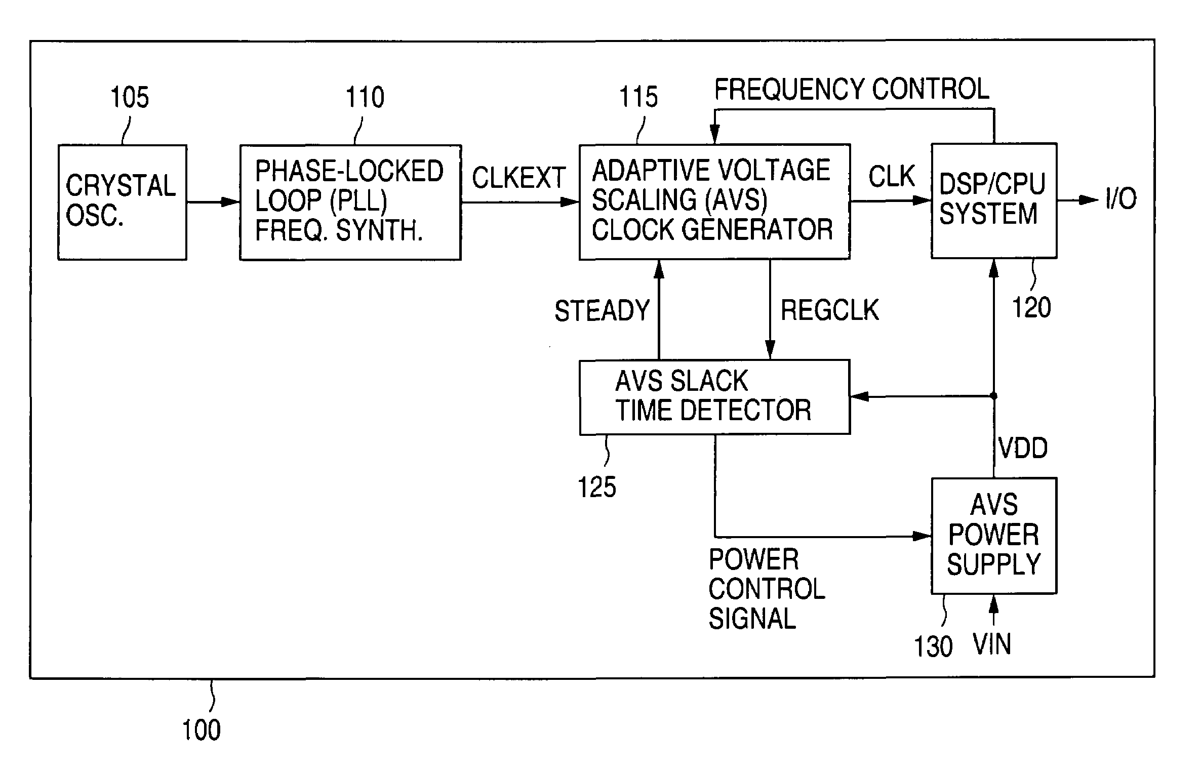
[0035]FIGS. 1 through 9, discussed below, and the various embodiments used to describe the principles of the present invention in this patent document are by way of illustration only and should not be construed in any way to limit the scope of the invention. Those skilled in the art will understand that the principles of the present invention may be implemented in any suitably arranged digital processing system.

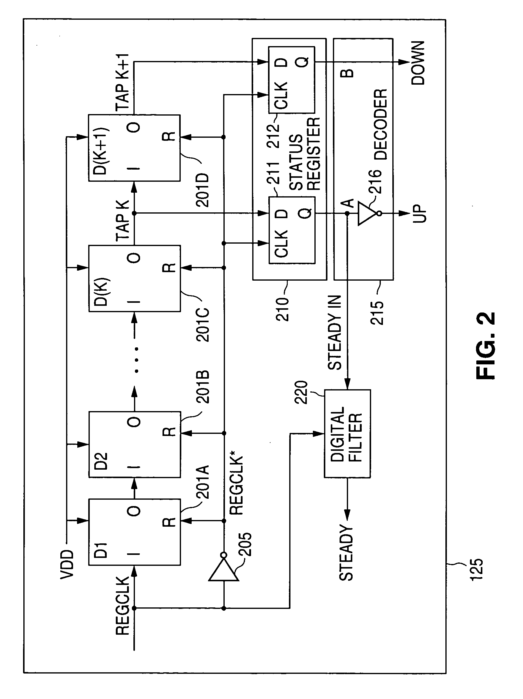
[0036]FIG. 1 illustrates a block diagram of digital processing system 100 according to one exemplary embodiment of the present invention. Digital processing system 100 comprises crystal oscillator 105, phase-locked loop (PLL) frequency synthesizer 110, adaptive voltage scaling (AVS) clock generator 115, a digital processing component, labeled DSP / CPU is system 120, adaptive voltage scaling (AVS) slack-time detector 125, and adaptive voltage scaling (AVS) power supply 130.

[0037]Exemplary crystal oscillator 105 generates an output reference frequency signal in which the referen...


PUM


Abstract

There is disclosed clock control circuitry for selectively applying a clock signal to a digital processing component wherein the clock signal is capable of being changed to a plurality of operating frequencies. The clock control circuitry is operable to (i) receive a command to change a first operating frequency to a second operating frequency, (ii) in response to the command, disable the applied clock signal, (iii) generate a test clock signal having the second operating frequency, (iv) apply the test clock signal to a power supply adjustment circuit, and (v) sense a status signal from the power supply adjustment circuit. The status signal indicates that a power supply level of the digital processing component has been adjusted to an optimum value suitable for the second operating frequency.

Description

CROSS-REFERENCE TO RELATED APPLICATIONS[0001]The present invention is related to those disclosed in the following U.S. patent applications:[0002]1. Ser. No. 10 / 053,226, filed concurrently herewith, entitled “AN ADAPTIVE VOLTAGE SCALING DIGITAL PROCESSING COMPONENT AND METHOD OF OPERATING THE SAME;”[0003]2. Ser. No. 10 / 053,858, filed concurrently herewith, entitled “SYSTEM FOR ADJUSTING A POWER SUPPLY LEVEL OF A DIGITAL PROCESSING COMPONENT AND METHOD OF OPERATING THE SAME;” and[0004]3. Ser. No. 10 / 053,228, filed concurrently herewith, entitled “AN ADAPTIVE VOLTAGE SCALING POWER SUPPLY FOR USE IN A DIGITAL PROCESSING COMPONENT AND METHOD OF OPERATING THE SAME,” now U.S. Pat. No. 6,548,991.[0005]The above applications are commonly assigned to the assignee of the present invention. The disclosures of these related patent applications are hereby incorporated by reference for all purposes as if fully set forth herein.TECHNICAL FIELD OF THE INVENTION[0006]The present invention is generall...

Claims


Application Information

Patent Timeline
IPC IPC(8): G06F1/32G06F1/08
CPCG06F1/08G06F1/3203G06F1/324G06F1/3296Y02B60/1217Y02B60/1285Y02D10/00
Inventor KRANZEN, BRUNOMAKSIMOVIC, DRAGAN
Owner NAT SEMICON CORP
Why Eureka
Try Eureka