Image sensing device using MOS type image sensing elements

a technology of image sensing and image sensing elements, which is applied in the direction of radio frequency control devices, instruments, television systems, etc., can solve the problems of mos type photoelectric conversion devices providing inferior images, affecting the linearity of input-output, and consuming a large amount of time to charge a capacitance with a small current, etc., to achieve good input-output linearity

Inactive Publication Date: 2005-09-20
CANON KK
View PDF19 Cites 119 Cited by
  • Summary
  • Abstract
  • Description
  • Claims
  • Application Information

AI Technical Summary

Benefits of technology

[0035]The present invention has been made in consideration of the above situation, and has as its object to provide a photoelectric conversion device having good input-output linearity.

Problems solved by technology

It has been said that a MOS type photoelectric conversion device provide an image of inferior quality compared to an image sensed by a CCD type photoelectric conversion device.
Further, when the current flowing through the source follower is reduced in order to reduce the voltage drop in the row selection switch 3, it takes considerable time to charge a capacitance with a small current.
Accordingly, it takes a considerable time to transfer signals, thus the number of pixels in the photoelectric conversion device is limited when charges should be transferred in a predetermined period.
Consequently, the conventional circuit is not suitable for operating a great number of pixels.
However, although the noise components are reduced, if the dynamic range of an element for reading photo-charge is narrow, the S / N ratio can not be further improved.
This makes the input dynamic range Dy unstable.
However, the conventional circuit can not meet the aforesaid demands of high resolution (more pixels), which causes an increase in driving load, and of low energy consumption (lower voltage), which causes deterioration of dynamic range.

Method used


Image

  • Image sensing device using MOS type image sensing elements
  • Image sensing device using MOS type image sensing elements
  • Image sensing device using MOS type image sensing elements

Examples


first embodiment

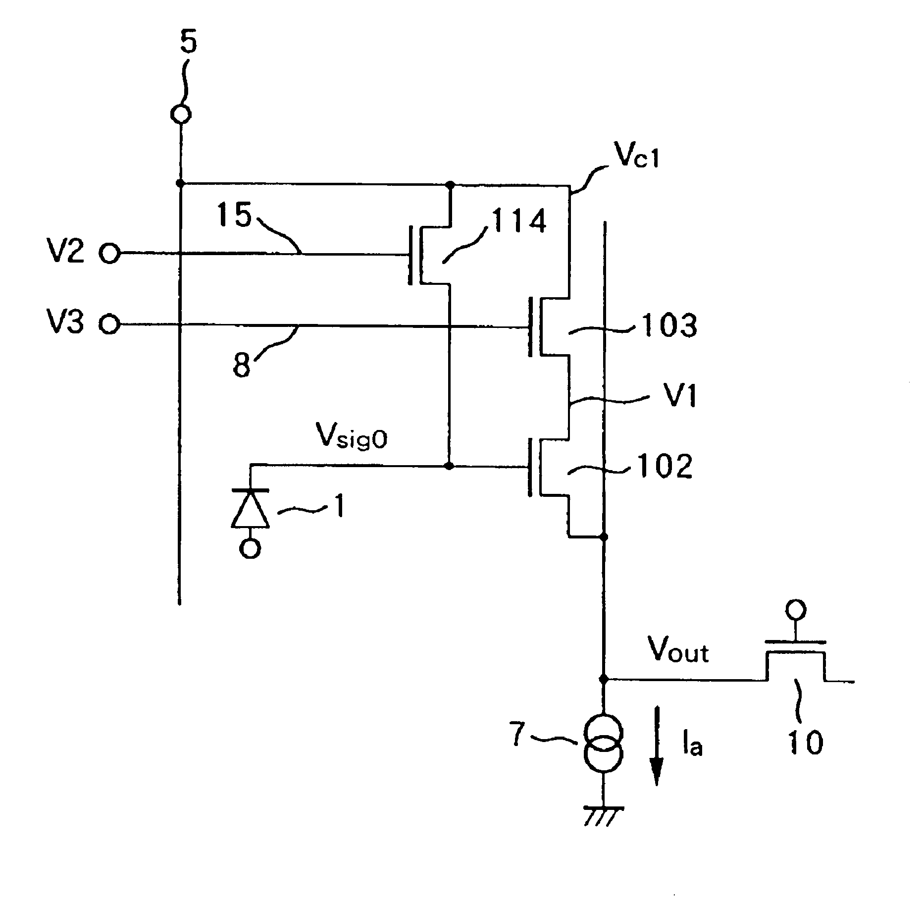
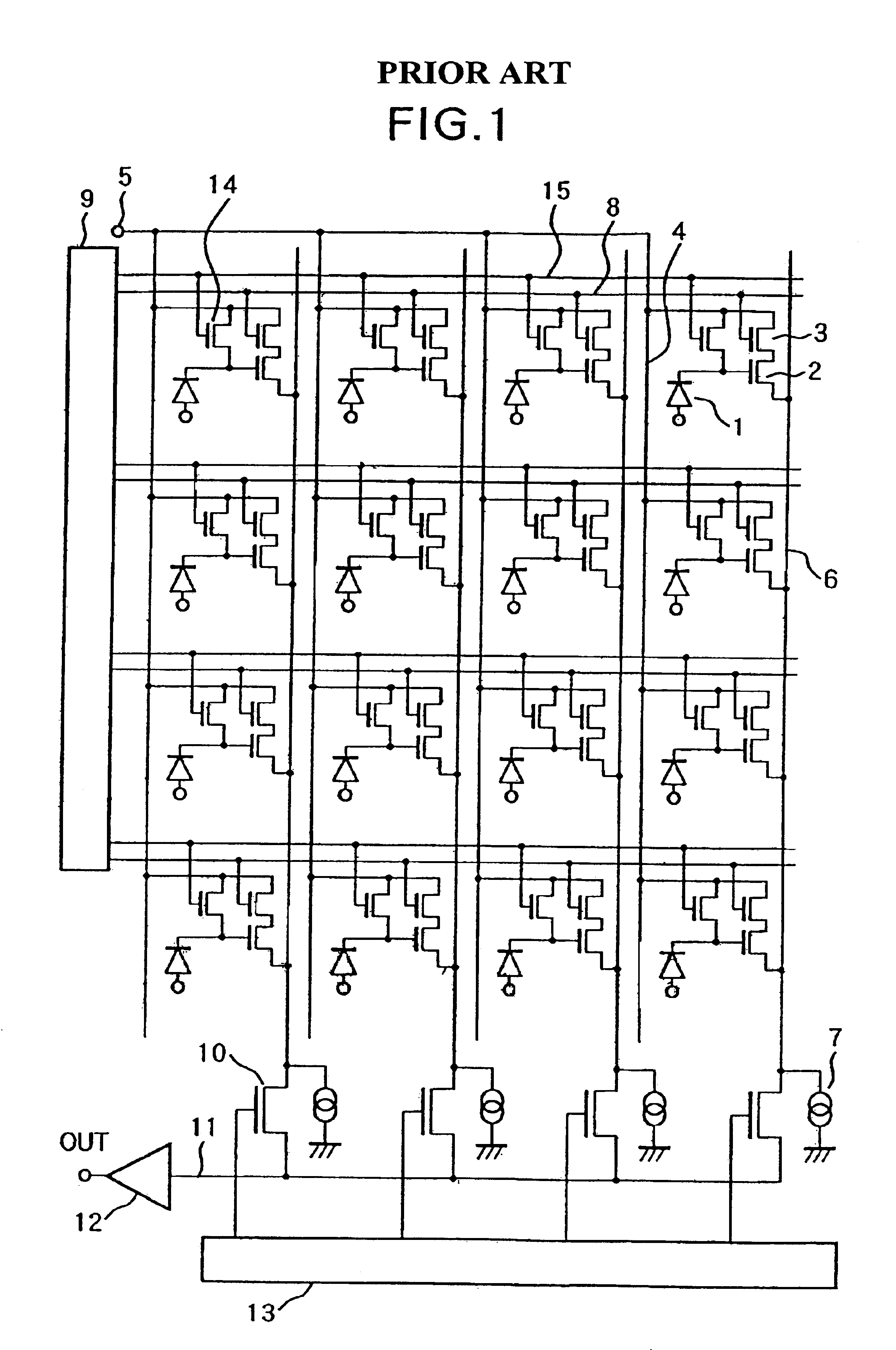
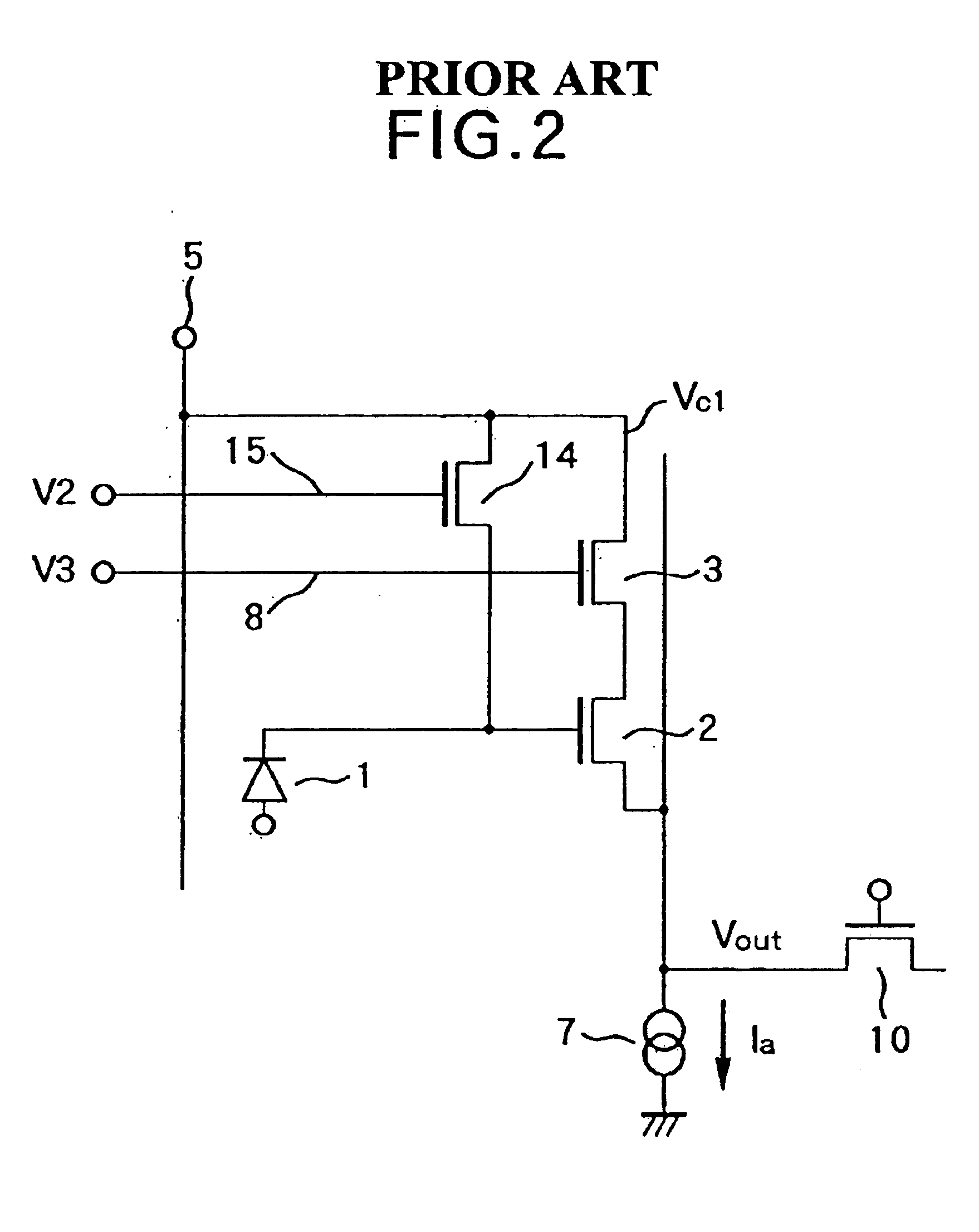
[0067]FIG. 6 is a circuit diagram showing one photoelectric conversion element 1 and its peripheral circuit corresponding to a single pixel according to the present invention. In FIG. 6, the MOS transistor 103 which acts as a row selection switch is a field effect transistor (FET). Let the gate voltage of the reset switch 114 when it is on be V2, the gate voltage of the row selection switch 103 when it is on be V3, the drain voltage of the MOS transistor 102 be V1, a threshold voltage of the reset switch 114 be Vth0, a threshold voltage of the row selection switch 103 be Vth1, and a threshold voltage of the MOS transistor 102 be Vth2. Note, the source follower is formed with the MOS transistors 102 and 103 and the constant current source 7.

[0068]As explained in the “Background of the Invention”, when the source follower operates in the linear operation region, the condition of the MOS transistors 103 and 102 to operate in the saturation region,

 Vds>Vgs−Vth   (1)

[0069]is satisfied...

second embodiment

[0089]In the second embodiment, a case where the MOS transistor 103 has a different threshold voltage from that of transistors 102 and 114 is explained.

[0090]As described in the first embodiment, when the MOS transistors 102, 103 and 104 have an identical threshold voltage, the current allowed to flow through the source follower is limited to a very low value. Therefore, when a higher resolution is demanded and a load that the source follower needs to drive increases, the configuration explained in the first embodiment can not meet the demand.

[0091]However, by setting the threshold voltage of the row selection switch 103 lower than those of the MOS transistors 102 and 114, it is possible to satisfy equation (12), or equation (1), while increasing the current Ia. When the voltages V2 and V3 applied to the gates of the reset switch 114 and the row selection switch 103 are the same (V2=V3), similarly to the first embodiment, by solving the equation (12) for (Ia / K)1 / 2, then the conditio...

fourth embodiment

[0128]As the fourth embodiment, a case where the reset switch 114 operates in the saturation region, and the row selection switch 103 operates in the linear region is explained. In this case, considering that the current flowing through the row selection switch 103 is the same as that flowing through the source follower, the following equation (21) is obtained with reference to FIG. 6.

Ia=K(V3−V1−Vth1)2−K(V3−Vc1−Vth1)2  (20)

[0129]where K=1 / 2×μ×Cox×W / L[0130]μ: Mobility[0131]Cox: Capacitance of gate oxide per unit area[0132]W: Gate width[0133]L: Gate length

[0134]By solving the equation (20) for V1, then

V1=V3−Vth1−(Ia / K+(V3−Vc1−Vth1)2)1 / 2  (21)

is obtained.

[0135]By plugging the equation (21) and the equation (9), shown in the first embodiment, into the equation (1), the condition for the source follower to operate in the linear operation region when the reset voltage Vsig0 is applied to the gate of the MOS transistor 102 is expressed as follows.

V3−Vth1−(Ia / K+(V3−Vc1−Vth1)2)1 / 2>V2−Vth...


PUM


Abstract

In a photoelectric conversion device having a plurality of pixel cells each of which includes a photoelectric conversion element, a field effect transistor having the gate area for storing signal charge generated by the photoelectric conversion element and the source-drain path for outputting a signal corresponding to the signal charge stored in the gate, a first power supply line for supplying electric power to the field effect transistor, and a first switch connected between the field effect transistor and the first power supply line, when a reset voltage for resetting the gate of the field effect transistor is Vsig0, a threshold voltage of the field effect transistor is Vth, current flowing through the field effect transistor is Ia, a voltage applied via the first power supply line is Vc1, and a series resistance of the first switch is Ron, each pixel cell is configured to satisfy a condition determined by Vc1−Ron×Ia>Vsig0−Vth.

Description

[0001]This application is a divisional of application Ser. No. 09 / 161,402, filed Sep. 28, 1998 now U.S. Pat. No. 6,670,990.BACKGROUND OF THE INVENTION[0002]The present invention relates to a photoelectric conversion device having a plurality of photoelectric conversion elements and, more particularly, to a photoelectric conversion device capable of improving linearity of the photoelectric conversion, further, widening a dynamic range by utilizing characteristics of transistors used for outputting signals corresponding to charges generated by photoelectric conversion elements and characteristics of metal-oxide semiconductor (MOS) transistor switches, thereby improving signal / noise (S / N) ratio.[0003]Conventionally, in a solid-state image sensing device, charge-coupled-device (CCD) type photoelectric conversion elements are used in most cases; however, MOS type photoelectric conversion elements have been recently developed for commercial products. It has been said that a MOS type photo...

Claims


Application Information

Patent Timeline
Patent Type & Authority Patents(United States)
IPC IPC(8): H01L27/146H04N3/15H04N5/355H04N5/363H04N5/365H04N5/374H04N5/3745
CPCH01L27/14609H01L27/14643H04N3/155H04N5/355H04N5/3559H04N5/363H04N5/365H04N5/374H04N5/3741H04N5/37452H04N25/59H04N25/67H04N25/65H04N25/766H04N25/771H04N25/76H01L27/146
Inventor KOCHI, TETSUNOBUSUGAWA, SHIGETOSHIUENO, ISAMUOGAWA, KATSUHISAKOIZUMI, TORUSAKURAI, KATSUHITOHIYAMA, HIROKI
Owner CANON KK
Why Eureka
Try Eureka