SONOS memory device having side gate stacks and method of manufacturing the same

a memory device and side gate technology, applied in the field of semiconductor memory devices, can solve the problems of difficult task, limited extent of such enhancement, and the degradation of yield in the semiconductor manufacturing process, and achieve the effect of high density storage and enhanced integration density of semiconductor memory devices

Inactive Publication Date: 2005-09-20
SAMSUNG ELECTRONICS CO LTD
View PDF1 Cites 59 Cited by
  • Summary
  • Abstract
  • Description
  • Claims
  • Application Information

AI Technical Summary

Benefits of technology

[0013]The present invention provides a silicon-oxide-nitride-oxide-silicon (SONOS) memory device that makes high-density storage possible while enhancing integration density of a semiconductor memory device without requiring scaling-down of memory device components.

Problems solved by technology

In most cases, reduction of the margins in the photo-etching process results in the degradation of yield in the semiconductor manufacturing process.
However, this is a difficult task because of limitations of an exposure process, such as a limitation of resolution.
As such, although the integration density of the conventional SONOS memory device may be enhanced as compared with the conventional memory cell, the extent of such enhancement is limited due to limitations of the exposure process.

Method used


Image

  • SONOS memory device having side gate stacks and method of manufacturing the same
  • SONOS memory device having side gate stacks and method of manufacturing the same
  • SONOS memory device having side gate stacks and method of manufacturing the same

Examples


first embodiment

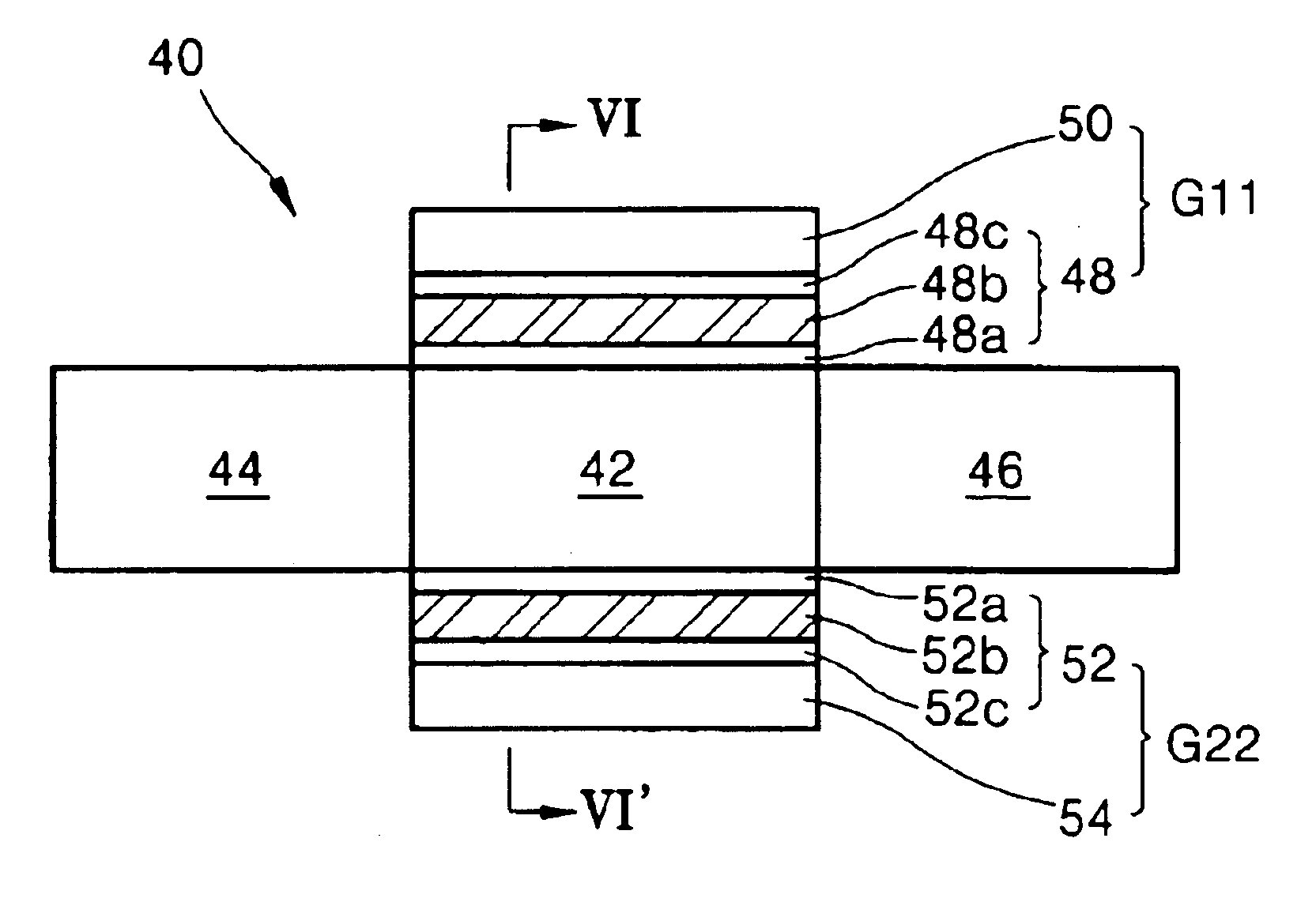
[0055]Referring to FIGS. 2 and 6, a SONOS memory device 40 according to the present invention includes an active layer that is deposited on a predetermined region of an insulating layer 72 formed on a semiconductor substrate 70. The insulating layer 72 is an oxide layer formed on the semiconductor substrate. The active layer is a semiconductor silicon layer. A channel region 42, a source region 44, and a drain region 46 are defined in the active layer. The channel region 42 is defined in a center of the active layer. The source region 44 is defined at one side of the channel region 42. The drain region 46 is defined at the other side of the channel region 42. Thus, the source region 44, the drain region 46, and the channel region 42 are defined in the same active layer. However, an impurity implanted into the source and drain regions 44 and 46 and a concentration thereof may be different from those of the channel region 42. For example, an n-type conductive impurity may be implanted...

second embodiment

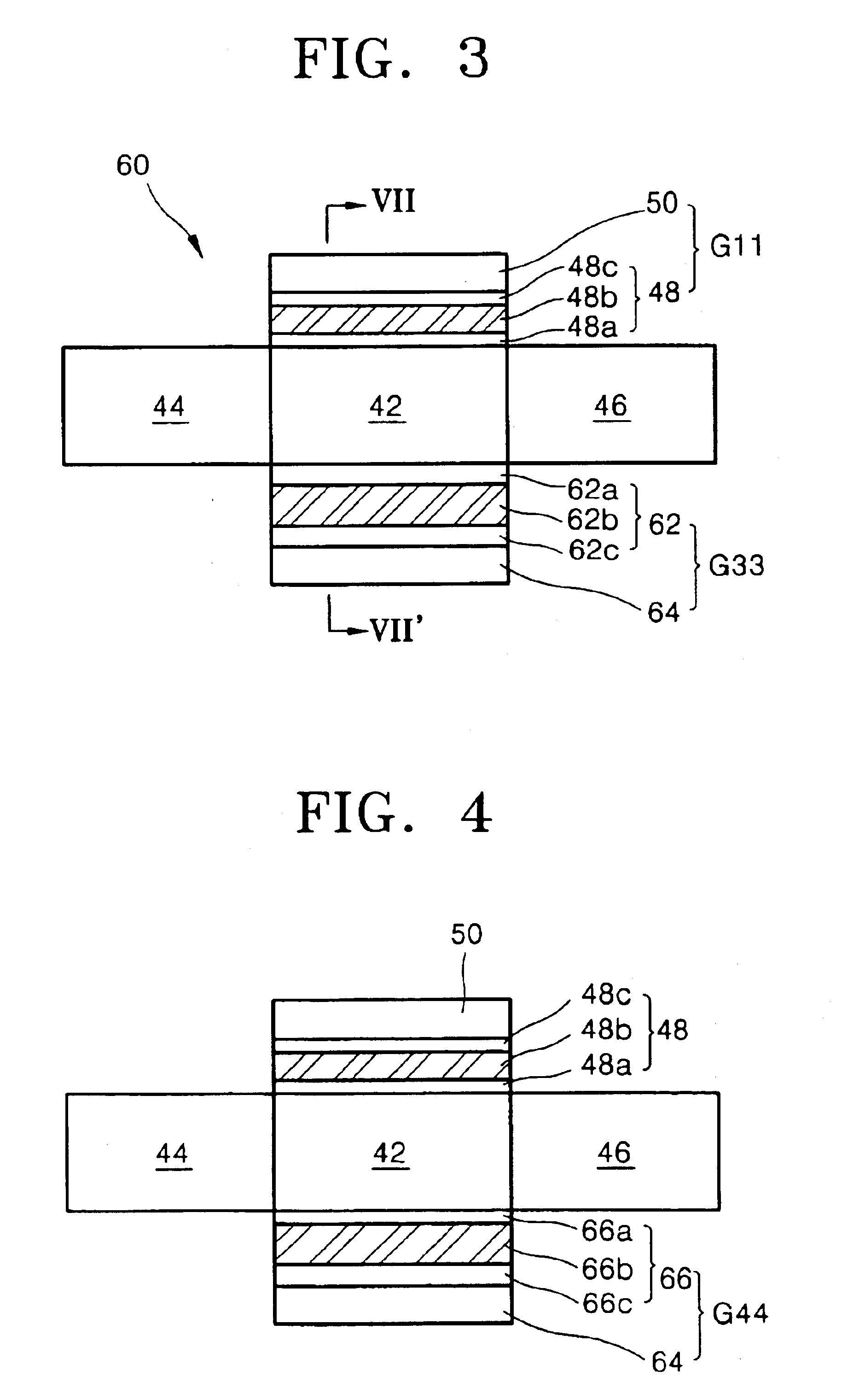
[0059]Referring to FIGS. 3 and 7, a SONOS memory device 60 according to the present invention includes a side gate stack G33 formed at the second side of the channel region 42. The side gate stack G33 includes a memory node 62 contacting the second side of the channel region 42 and a side gate conductive layer 64 formed at a side of the side gate stack G33. The memory node 62 includes a tunneling oxide layer 62a, a trapping layer 62b, and a blocking oxide layer 62c, which are sequentially formed at the second side of the channel region 42. Here, the thickness of the tunneling oxide layer 62a is greater than that of the first tunneling oxide layer 48a. The thickness of the trapping layer 62b is greater than that of the first trapping layer 48b. The thickness of the blocking oxide layer 62c is greater than that of the first blocking oxide layer 48c.

[0060]Since the thicknesses of the tunneling oxide layer 62a, the trapping layer 62b, and the blocking oxide layer 62c are respectively d...

third embodiment

[0065]In the present invention, a SONOS memory device includes two side gate stacks and one vertical gate stack that share a material layer used as a memory node.

[0066]Referring to FIG. 8, the insulating layer 72 is formed on the semiconductor substrate 70. The channel region 42 is formed on a predetermined region of the insulating layer 72. All exposed surfaces of the channel region 42, that is, side surfaces and a top surface of the channel region 42 are covered with a tunneling oxide layer 74. All exposed surfaces of the tunneling oxide layer 74 are covered with a trapping layer 76. All exposed surfaces of the trapping layer 76 are covered with a blocking oxide layer 78. The tunneling oxide layer 74, the trapping layer 76, and the blocking oxide layer 78 constitute a memory node including a first part N1, a second part N2, and a third part N3 that cover exposed surfaces of the channel region 42. First and second conductive layers 80 and 82 are formed at first and second sides of ...


PUM


Abstract

In a silicon-oxide-nitride-oxide-silicon (SONOS) memory device and a method of manufacturing the same, a SONOS memory device includes a semiconductor substrate, an insulating layer deposited on the semiconductor substrate, an active layer formed on a predetermined region of the insulating layer and divided into a source region, a drain region, and a channel region, a first side gate stack formed at a first side of the channel region, and a second side gate stack formed at a second side of the channel region opposite the first side of the channel region. In the SONOS memory device, at least two bits of data may be stored in each SONOS memory device, thereby allowing the integration density of the semiconductor memory device to be increased without increasing an area thereof.

Description

BACKGROUND OF THE INVENTION[0001]1. Field of the Invention[0002]The present invention relates to a semiconductor memory device and a method of manufacturing the same. More particularly, the present invention relates to a silicon-oxide-nitride-oxide-silicon (SONOS) memory device having an enhanced integration density without increasing an area of the semiconductor memory device and a method of manufacturing the same.[0003]2. Description of the Related Art[0004]Data storage capacity of a semiconductor memory device is proportional to the number of memory cells per unit area, or integration density, of the device.[0005]Typically, each memory cell consists of one transistor and one capacitor. Therefore, it is possible to enhance the integration density of a semiconductor memory device by scaling-down a size of the transistor and the capacitor. Since early semiconductor memory devices of low integration density have sufficient margins for a photo-etching process, scaling-down of transist...

Claims


Application Information

Patent Timeline
Patent Type & Authority Patents(United States)
IPC IPC(8): H01L21/28H01L29/66H01L21/336H01L21/02H01L29/792H01L21/8247H01L27/115H01L29/423H01L29/788
CPCH01L21/28273H01L21/28282H01L29/42328H01L29/66833H01L29/7881H01L29/792H01L29/7923H01L29/40114H01L29/40117B82Y10/00H10B69/00
Inventor RYU, WON-ILLEE, JO-WONYOON, SE-WOOKKIM, CHUNG-WOO
Owner SAMSUNG ELECTRONICS CO LTD
Why Eureka
Try Eureka