

Multiple data rate interface architecture
- Summary
- Abstract
- Description
- Claims
- Application Information
AI Technical Summary
Benefits of technology
Problems solved by technology
Method used
Image

Examples
Embodiment Construction
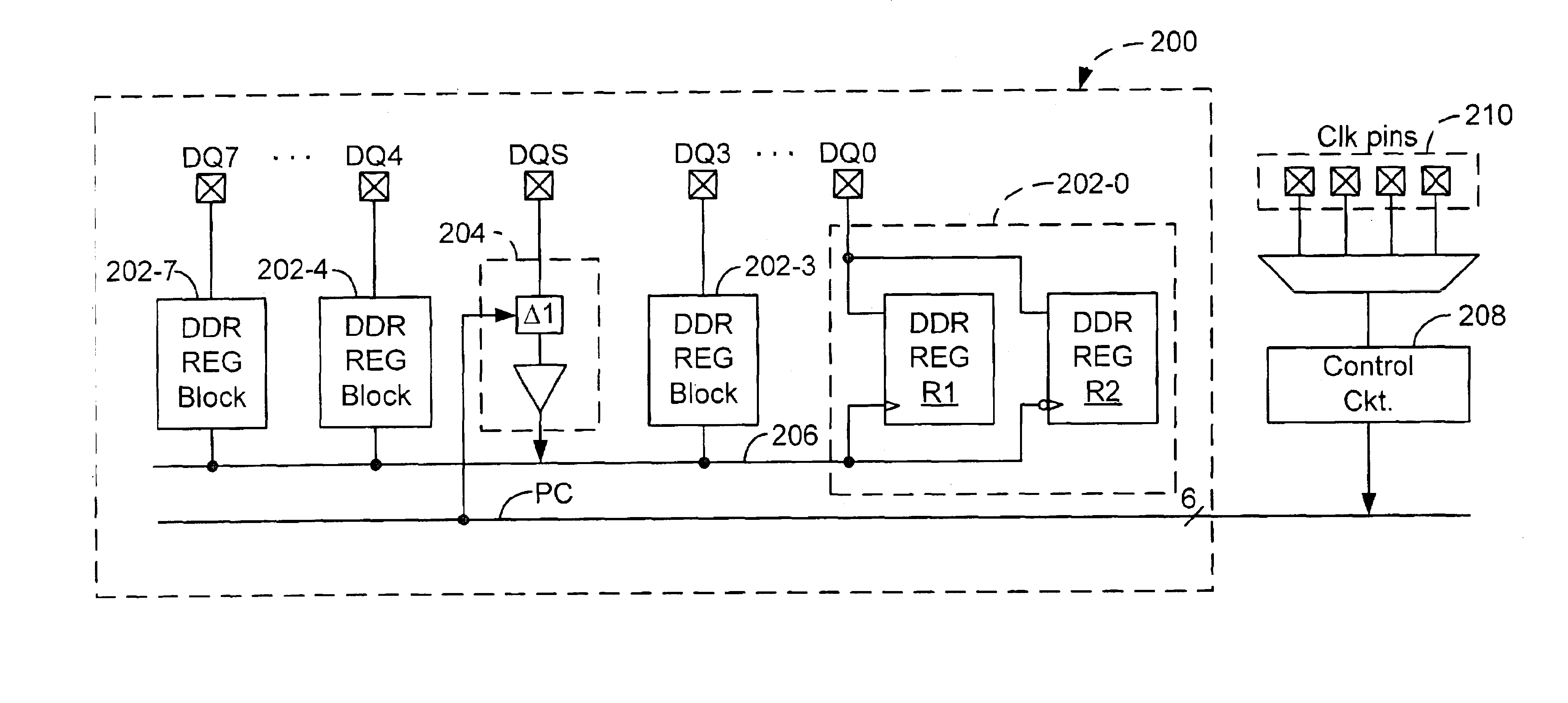
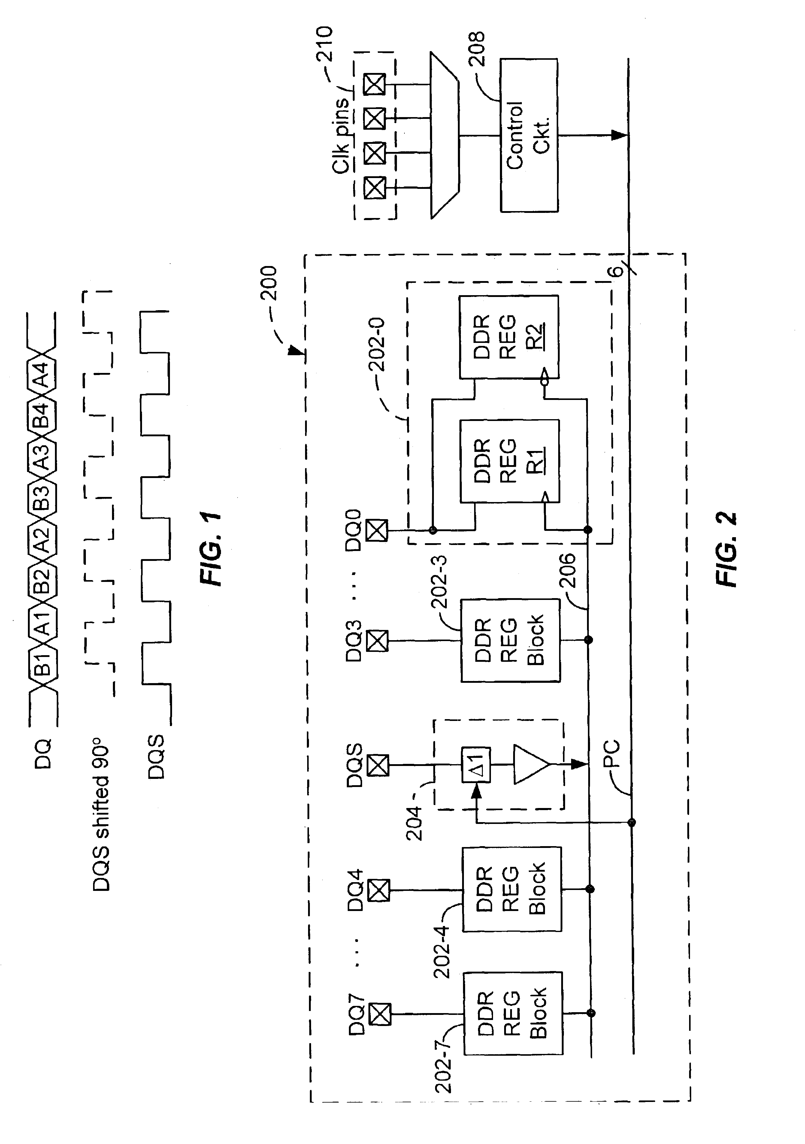
[0018]To minimize skew, accommodate a wide frequency range of operation, and facilitate rapid pin migration to larger PLDs, the present invention provides a modular multiple-data-rate I / O architecture that can be readily replicated and scaled. For illustrative purposes, the invention is described in the context of a double-data rate (DDR) system. It is to be understood, however, that the principles of this invention can be applied to systems operating at quad-data rate or higher. Referring to FIG. 2, there is shown a block diagram of an I / O module 200 for a PLD configured for DDR operation according to one embodiment of the present invention. In this embodiment, DDR interface module 200 includes a number of, in this example eight, data I / O cells each having a data I / O pin DQ and a DDR register block 202 made up of a pair of data registers R1 and R2. Module 200 also includes a strobe input cell which is preferably located at a central location vis á vis other I / O cells, and includes ...
PUM
 Abstract
Description
Claims
Application Information