Solid-state imaging device with dynamic range control

a solid-state imaging and dynamic range technology, applied in the direction of radio frequency controlled devices, television system scanning details, etc., can solve the problems of low dynamic, inability to perform electronic shutter operation for controlling exposure time, uneven reset potential of vertical signal line vlin of its other end, etc., to achieve a good image and increase the dynamic range of amplification-type cmos image sensor.

Inactive Publication Date: 2005-09-20
KK TOSHIBA
View PDF22 Cites 32 Cited by
  • Summary
  • Abstract
  • Description
  • Claims
  • Application Information

AI Technical Summary

Benefits of technology

[0042]The present invention has been made to eliminate the above problems, and it is an object of the present invention to provide a solid-state imaging device capable

Problems solved by technology

However, the gate potential of the amplifying transistor Tb of the unit cell 1 of one row reset here is changed, and the reset potential of the vertical signal line VLIN of its other end with become uneven.
Namely, as the photodiode PD discharges the stored charges only one by one field, it is impossible to perform an electronic shutter operation for controlling the exp

Method used


Image

  • Solid-state imaging device with dynamic range control
  • Solid-state imaging device with dynamic range control
  • Solid-state imaging device with dynamic range control

Examples


first embodiment

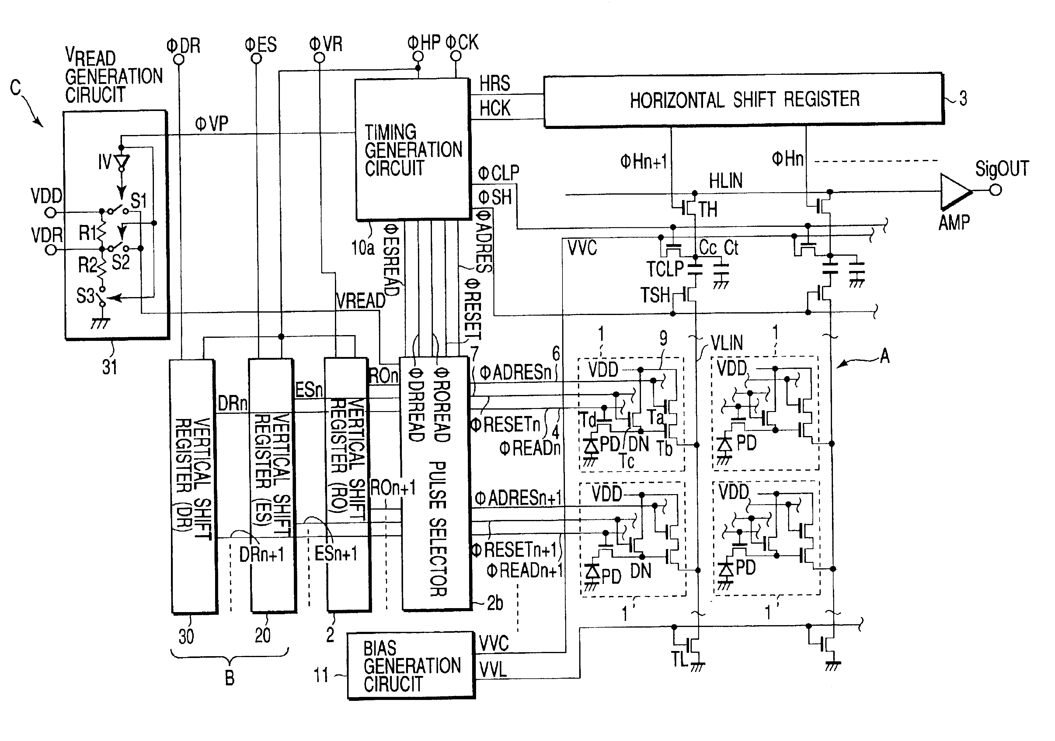
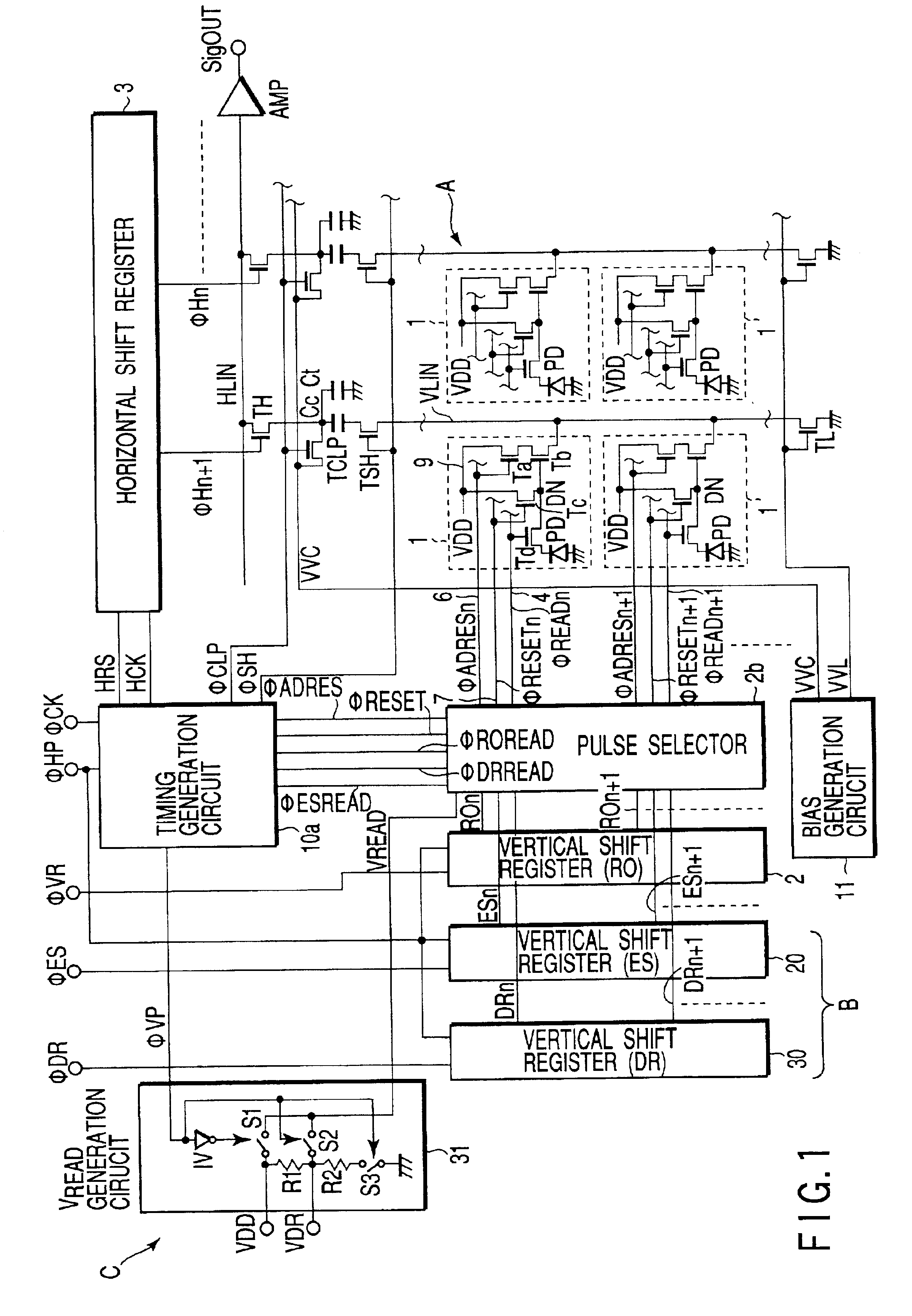
[0062]FIG. 1 is a block diagram showing schematically an amplification type CMOS image sensor according to the present invention.

[0063]Compared to the CMOS image sensor shown in FIG. 12, the CMOS image sensor of FIG. 1 is mostly similar to except the following points, and those same as in FIG. 12 have the same reference numerals.

[0064](1) A vertical shift register 30 is provided for generating sequentially pulses DRi (i=. . . , n, n+1, . . . ) of a dynamic range control, based on the external input pulse φDR.

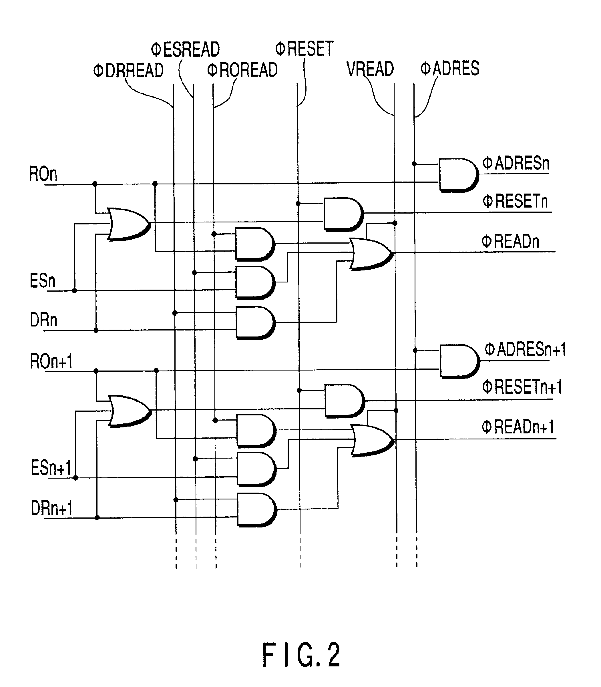
[0065]Namely, the image sensor includes a pulse generation circuit B comprised of three vertical shift registers 2, 20, 30 for producing three pulses ESi, DRi, ROi for respective pixel rows, as a pulse signal source for controlling the readout timing in the readout transistor Td.

[0066](2) A voltage VDR of a readout driving signal is applied to the readout transistor Td corresponding to the pulse DRi of the dynamic range control. In order to set the voltage VDR to a lower voltage...

second embodiment

[0133]FIG. 8 shows schematically a circuit structure of an amplification type CMOS image sensor according to the present invention.

[0134]This CMOS image sensor includes an AD conversion circuit 21 having a noise reduction function, and converts analog signal transmitted to a plurality of vertical signal line VLIN into digital signals by the AD conversion circuit 21 to provide output signals.

[0135]Now, points different from the CMOS image sensor shown in FIG. 1 will be described mainly.

[0136]Namely, in the AD conversion circuit 21 of the CMOS image sensor shown in FIG. 8, a comparator CMP connected to one end of the vertical signal line VLIN for each pixel column is disposed in the horizontal direction. This comparator CMP compares analog signals from the vertical signal line VLIN with the reference signal VREF provided from the reference signal generation circuit 22. This reference signal VREF is, basically, a RAMP wave whose voltage increases with the lapse of time. The comparator ...


PUM


Abstract

A solid-state imaging device includes unit cells, arranged in a matrix of rows and columns, each having a photodiode for photoelectrically converting incident light to store signal charges, a readout transistor Td for reading out the signal charges and amplifying transistor Tb for amplifying signals readout at a detection node, a plurality of vertical shift registers for generating signal charge readout pulses ESi, DRi, ROi and a voltage switching circuit for setting a voltage VDR of the readout pulse DRi for dynamic range control lower than voltages of both a readout pulse ESi for an electronic shutter and a usual readout pulse ROi. The solid-state imaging device provides excellent images without clipping from a small signal region to large signal region.

Description

CROSS-REFERENCE TO RELATED APPLICATIONS[0001]This application is based upon and claims the benefit of priority from the prior Japanese Patent Application No. 11-375475, filed Dec. 28, 1999, the entire contents of which are incorporated herein by reference.BACKGROUND OF THE INVENTION[0002]The present invention relates to an amplification type solid-state imaging device for amplifying and extracting signals obtained by photoelectric conversion means, and especially a pixel signal readout driving circuit of CMOS type image sensor, which can be used for video cameras, electric still cameras or the like capable of electronic shutter control operation.[0003]In recent years, the amplification type CMOS image sensor, known as solid-state imaging device appropriate for the application to video cameras, electric still cameras or the like, has a structure to amplify and extract signals obtained by the photoelectric conversion means for each cell by a MOS transistor. To be more specific, the ch...

Claims


Application Information

Patent Timeline
IPC IPC(8): H01L27/146H04N3/15H01L21/339H01L29/762H04N5/335H04N5/353H04N5/355H04N5/369H04N5/374H04N5/3745
CPCH01L27/14643H04N3/155H04N25/575H04N25/745H04N25/77
Inventor EGAWA, YOSHITAKAOHSAWA, SHINJIENDO, YUKIONAKAMURA, NOBUO
Owner KK TOSHIBA
Why Eureka
Try Eureka