

Flip chip package with warpage control
- Summary
- Abstract
- Description
- Claims
- Application Information
AI Technical Summary
Benefits of technology
Problems solved by technology
Method used
Image

Examples
example
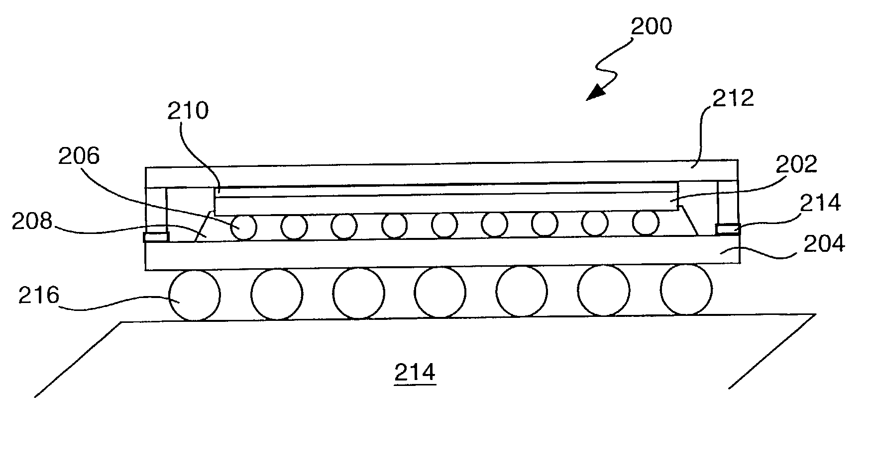
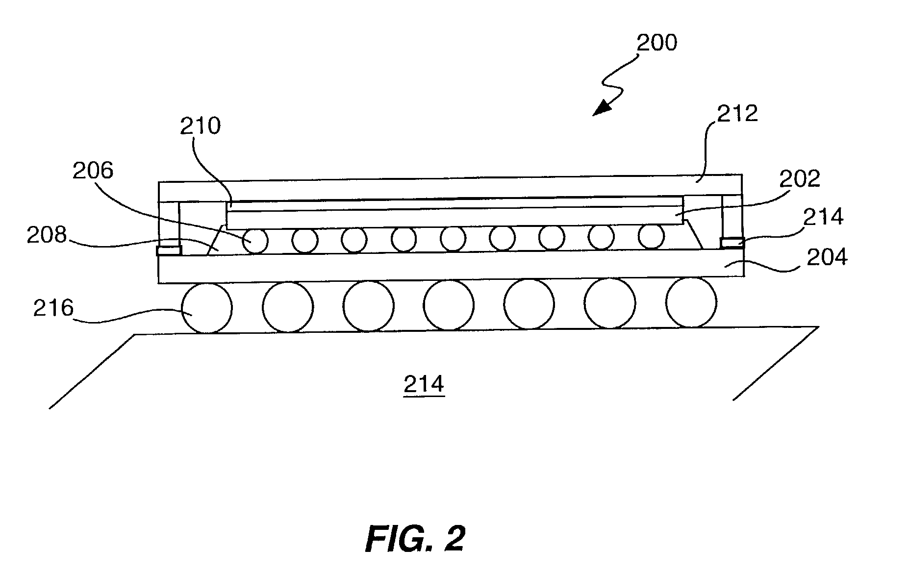
[0039]The following example provides details concerning semiconductor flip chip packages with warpage control in accordance with one embodiment of the present invention. It should be understood the following is representative only, and that the invention is not limited by the detail set forth in this example.
[0040]A multilayer organic (BT) package having a surface preparation including a solder mask material, and pre-applied solder surfaces to enhance the mounting of the chip to the package was provided. The die was position in registration to the pads of pre-applied eutectic solder (63 / 37 PbSn) and subjected to a thermal excursion above 200° C. to reflow the eutectic solder to the high lead (95 / 5 PbSn) solder bumps on the die. The die was then underfilled with a low modulus thermoset material (Namics 8439-1), which had suitable thermal characteristics to improve the thermal cycling reliability of the solder bumps of the attached chip. After underfill, a suitable window frame compos...
PUM
 Abstract
Description
Claims
Application Information