Electron beam apparatus

a technology of electron beam and apparatus, applied in the direction of beam deviation/focusing, instruments, heat measurement, etc., can solve the problems of high apparatus manufacturing cost, falling efficiency with which secondary electrons are detected, and affecting image resolution

Inactive Publication Date: 2005-09-27
HITACHI HIGH TECH SCI CORP
View PDF21 Cites 6 Cited by
  • Summary
  • Abstract
  • Description
  • Claims
  • Application Information

AI Technical Summary

Benefits of technology

[0013]In order to resolve the aforementioned problems, according to the present invention, there is provided an electron beam apparatus equipped with a magnetic field lens arranged on the same axis as an optical axis and configured in such a manner that an electron beam from an electron beam source advancing along the optical axis and being incident to the magnetic field lens focused onto a sample subjected to a negative voltage, with electrons emitted from the sample as a result of the sample being irradiated with the electron beam being detected, wherein a conductive cylinder is arranged so a...

Problems solved by technology

As a result, there is a problem where the efficiency with which secondary electrons are detected falls.
The intensity of the electromagnetic field of the Wien filter is therefore large, and the influence of Wien filter aberrations on the beam therefore easily becomes large which can easily prove detrimental to image resolution.
In addition to making the apparatus manufacturing costs high, this also makes the electron beam apparatus as a whole large, which results in an expensive product.
This means that detection efficiency is not sufficient.
Further, a deflector is provided in order to perform beam scanning on the sample surface but the amount of secondary electrons deflected depends on the strength of the deflector and there is therefore a further problem in that it is easy for the center of the screen to become dark.
It has therefore been difficult to set the strength of the deflectors appropriately so as to obtain a sufficient secondary electr...

Method used


Image

  • Electron beam apparatus
  • Electron beam apparatus
  • Electron beam apparatus

Examples


Embodiment Construction

[0033]Embodiments of the present invention will be described in more detail below with reference to the drawings.

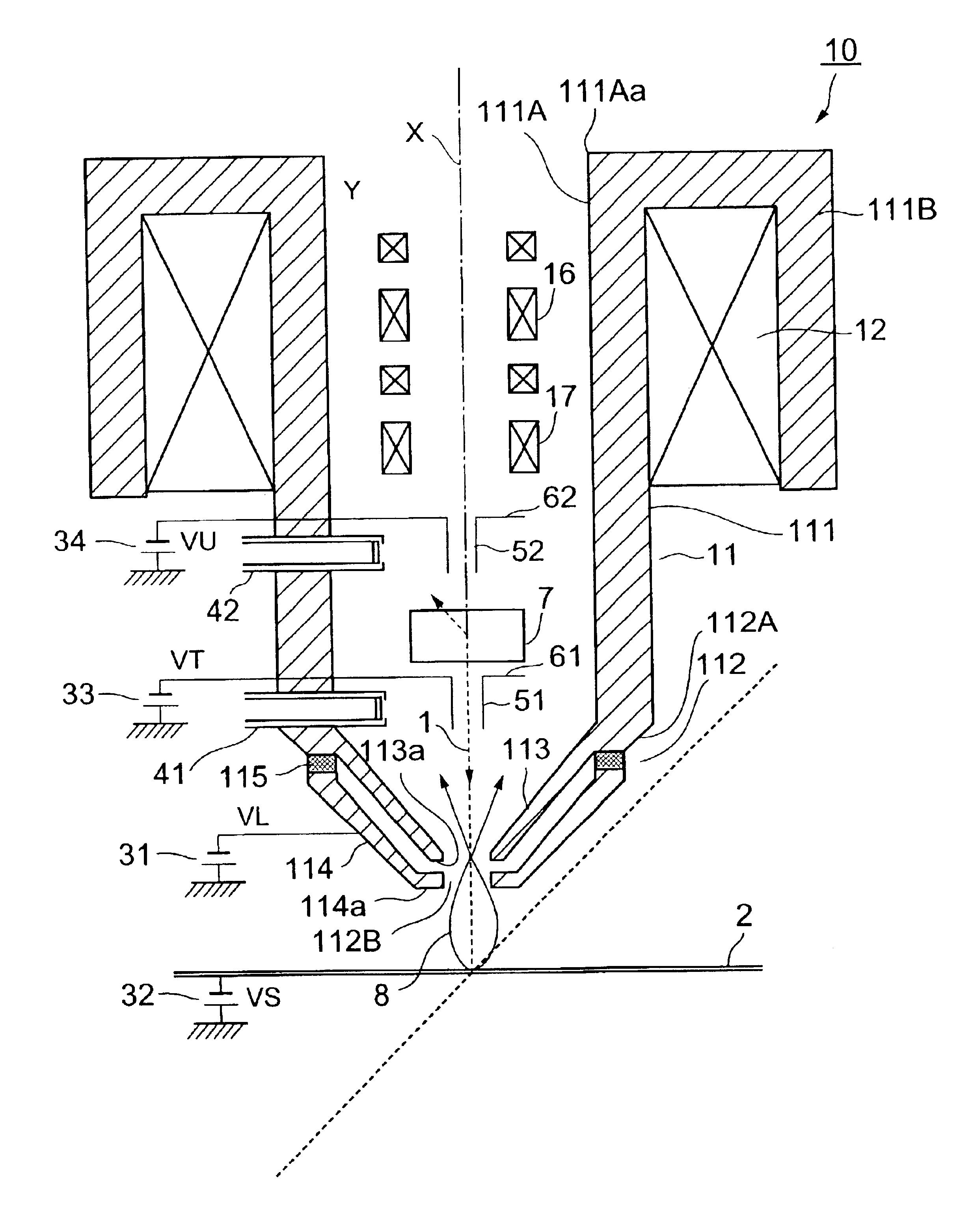
[0034]FIG. 1 is a cross-sectional view of an example of an embodiment of a single pole-piece lens with an electrostatic bipotential lens 10 of the present invention provided in an electron beam apparatus (not shown) . The single pole-piece lens with an electrostatic bipotential lens 10 is configured as an objective lens of the electronic apparatus, such as a scanning electron microscope apparatus, used in scanning and observation of the shapes of fine pattern electronic devices, and subjects an electron beam 1 advancing along an optical axis X from an electron gun (not shown) to the focusing action of a magnetic field and superimposes a decelerating electric field with the magnetic field so as to reduce the chromatic aberration coefficient of the lens in order to provide an electrostatic magnetic objective lens capable of narrowly focusing the electron beam 1 onto the sam...


PUM


Abstract

An electron beam apparatus has an optical axis, an electron beam source for generating an electron beam directed along the optical axis, and a magnetic field lens having an axis coincident with the optical axis for focusing the electron beam onto a sample which is subjected to a negative voltage so that secondary electrons are emitted from the sample. The magnetic field lens has a conductive cylinder surrounding a part of the optical axis to permit the passage therethrough of an electron beam from the electron beam source. A first detector detects secondary electrons emitted by the sample in a direction away from the optical axis and is disposed at a position generally confronting the conductive cylinder. A second detector is disposed over the conductive cylinder. A Wien filter deflector deflects secondary electrons emitted by the sample toward and for detection by the second detector. The Wien filter deflector is disposed on the optical axis and between the conductive cylinder and the second detector.

Description


Claims


Application Information

Patent Timeline
IPC IPC(8): H01J37/28H01J37/244H01J37/145
CPCH01J37/10H01J37/244H01J37/28H01J2237/2449
Inventor YONEZAWA, AKIRA
Owner HITACHI HIGH TECH SCI CORP
Why Eureka
Try Eureka