Stacked gate region of a memory cell in a memory device

a memory cell and gate region technology, applied in the field of polysilicon structures in the stacked gate region of a semiconductor device, can solve the problems of difficult to reduce the size or scale down achieve the effect of increasing the capacitive coupling of the memory cell, reducing or scaling the size of the memory cell and the devi

Inactive Publication Date: 2005-09-27
MICRON TECH INC
View PDF31 Cites 5 Cited by
  • Summary
  • Abstract
  • Description
  • Claims
  • Application Information

AI Technical Summary

Benefits of technology

[0007]The present invention includes polysilicon wings or ears which can increase the capacitive coupling of memory cells in memory devices in which they are used. Generally, the polysilicon wings or ears are placed proximate to the floating gate of a memory cell. Thus, the present invention may allow for further reducing or scaling the size of memory cells and devices.

Problems solved by technology

It is difficult to reduce the size or scale down the memory cell while maintaining a desired or required capacitive coupling.

Method used


Image

  • Stacked gate region of a memory cell in a memory device
  • Stacked gate region of a memory cell in a memory device
  • Stacked gate region of a memory cell in a memory device

Examples


Embodiment Construction

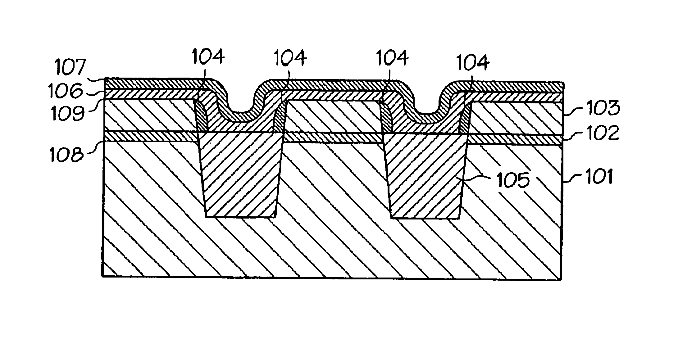
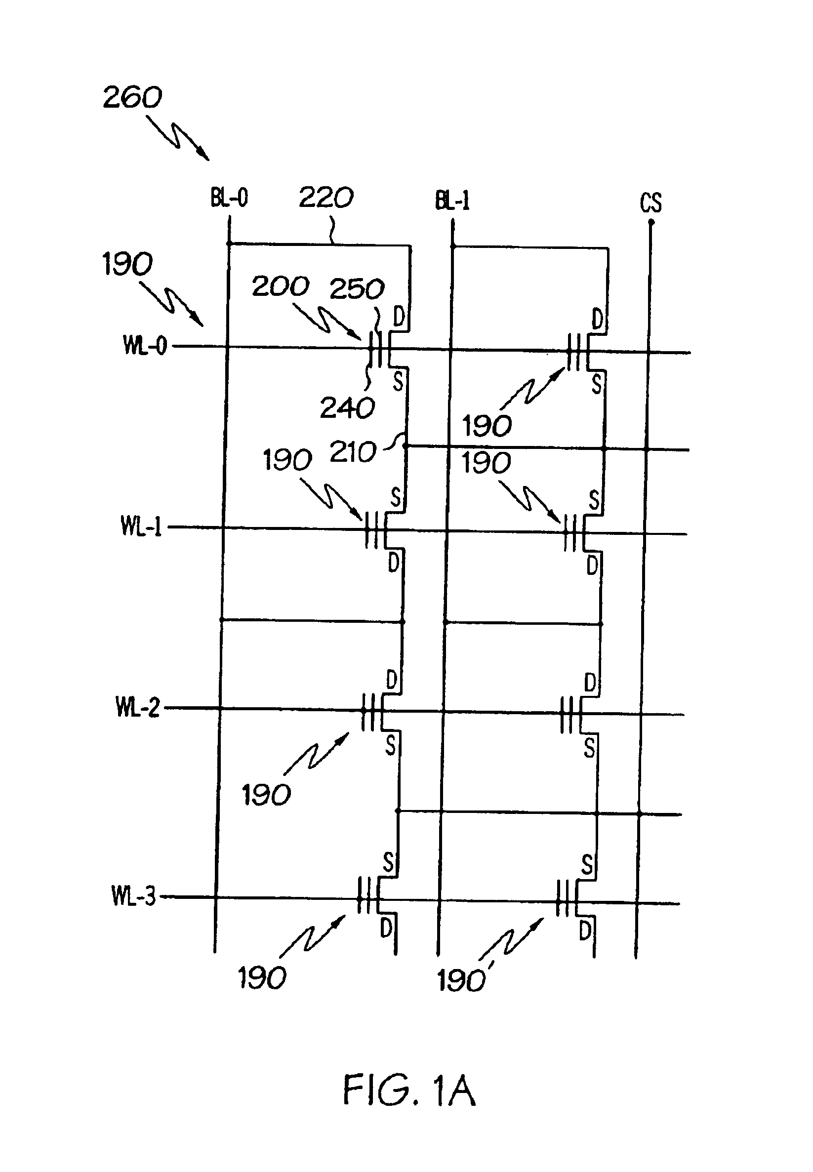
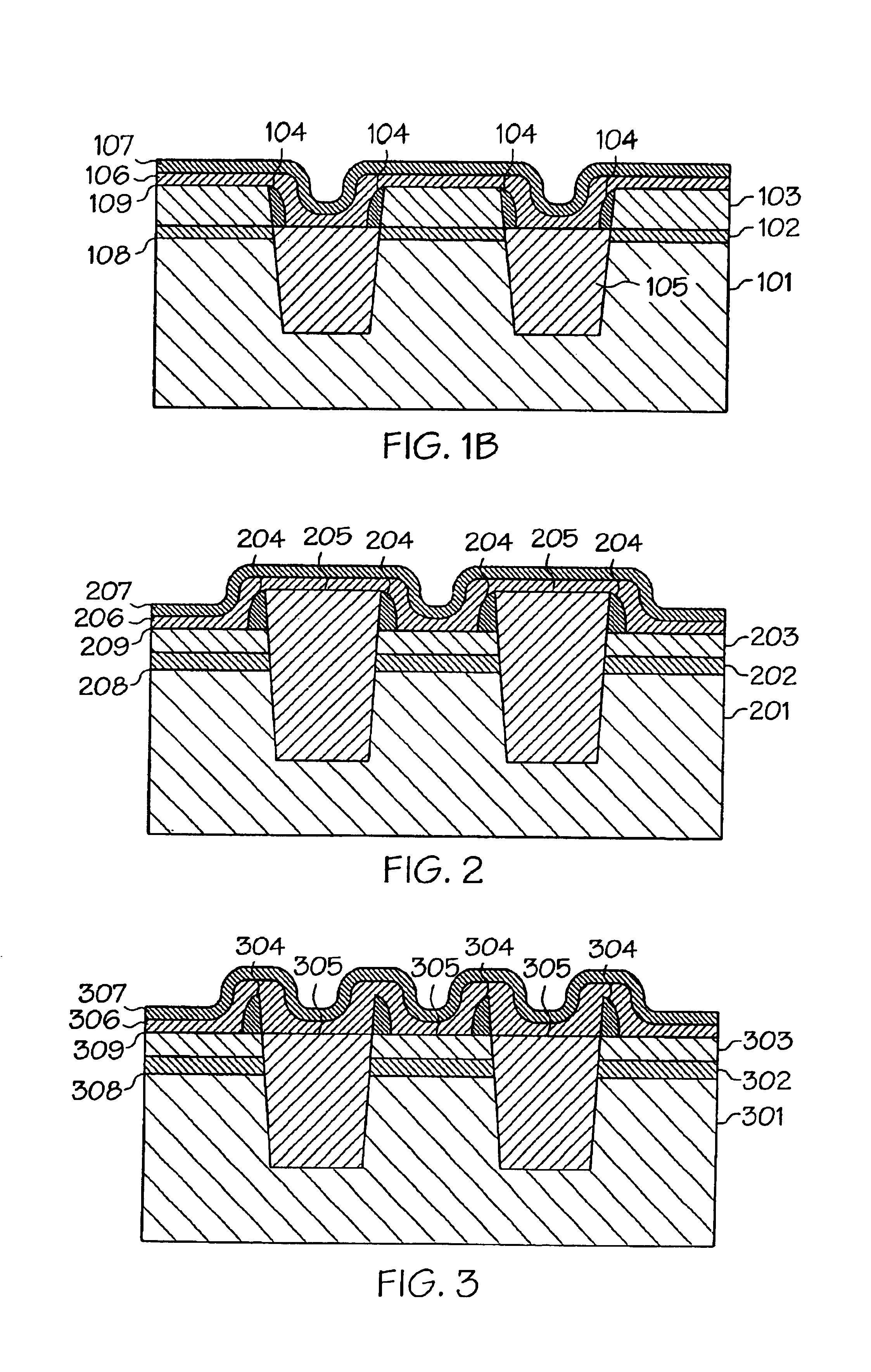
[0055]FIG. 1A illustrates a memory array 260 according to one embodiment of the invention. The memory array 260 includes a plurality of memory cells 190. Each memory cell 190 includes a source 210, drain 220 and a stacked gate region or gate structure 200. The gate structure 200 includes a floating gate 250 and a control gate 240. The floating gate 250 includes polysilicon wings or ears, described in further detail herein, which increase the capacitive coupling of the memory cell 190. The control gates 240 of the respective cells 190 in a row are formed integral to a common word line (WL) associated with the row. In the completed memory array, the source 210 of each memory cell 190 in a column is formed in a common region with the source 210 of one of the adjacent memory cells. Similarly, the drain 220 of each memory cell is formed in a common region with the drain 220 of another adjacent memory cell. Additionally, the sources 210 of each memory cell 190 in a row, and hence pair of ...


PUM


Abstract

Semiconductor devices are disclosed utilizing at least one polysilicon structure in a stacked gate region according to the present invention. The stacked gate region includes a substrate, at least one trench, an oxide layer, at least one floating gate layer and the at least one polysilicon structure. The at least one polysilicon structure is formed adjacent to vertical edges of the at least one floating gate layer and above the oxide layer. The polysilicon structure, which includes polysilicon wings and ears, is used to increase the capacitive coupling of memory cells in memory devices, thereby allowing for further reduction or scaling in the size of memory cells and devices.

Description

CROSS REFERENCE TO RELATED APPLICATIONS[0001]This application is a continuation of U.S. patent application Ser. No. 10,273,053 filed Oct. 17, 2002, now U.S. Pat. No. 6,759,708 which is a division of U.S. patent application Ser. No. 09 / 808,484 filed Mar. 14, 2001 (abandoned).BACKGROUND OF THE INVENTION[0002]The present invention relates to the field of semiconductor manufacture and, more particularly, to polysilicon structures in a stacked gate region of a semiconductor device, such as for example, a flash memory device. As computers become increasingly complex, the need for improved memory storage, and in particular, the need for an increased number of memory cells per unit area, increases. At the same time, there is a continuing drive to minimize the size of computers and memory devices. Accordingly, it is a goal of memory device fabrication to increase the number of memory cells per unit area or wafer area.[0003]A conventional non-volatile semiconductor memory device in which cont...

Claims


Application Information

Patent Timeline
Patent Type & Authority Patents(United States)
IPC IPC(8): H01L21/70H01L27/115H01L21/8247
CPCH01L27/115H01L27/11521H10B69/00H10B41/30
Inventor HURLEY, KELLY T.WOLSTENHOLME, GRAHAM
Owner MICRON TECH INC
Why Eureka
Try Eureka