
Method for using a hard mask for critical dimension growth containment

Inactive Publication Date: 2005-10-04
SPTS TECH LTD
View PDF11 Cites 0 Cited by
  • Summary
  • Abstract
  • Description
  • Claims
  • Application Information

AI Technical Summary

Benefits of technology

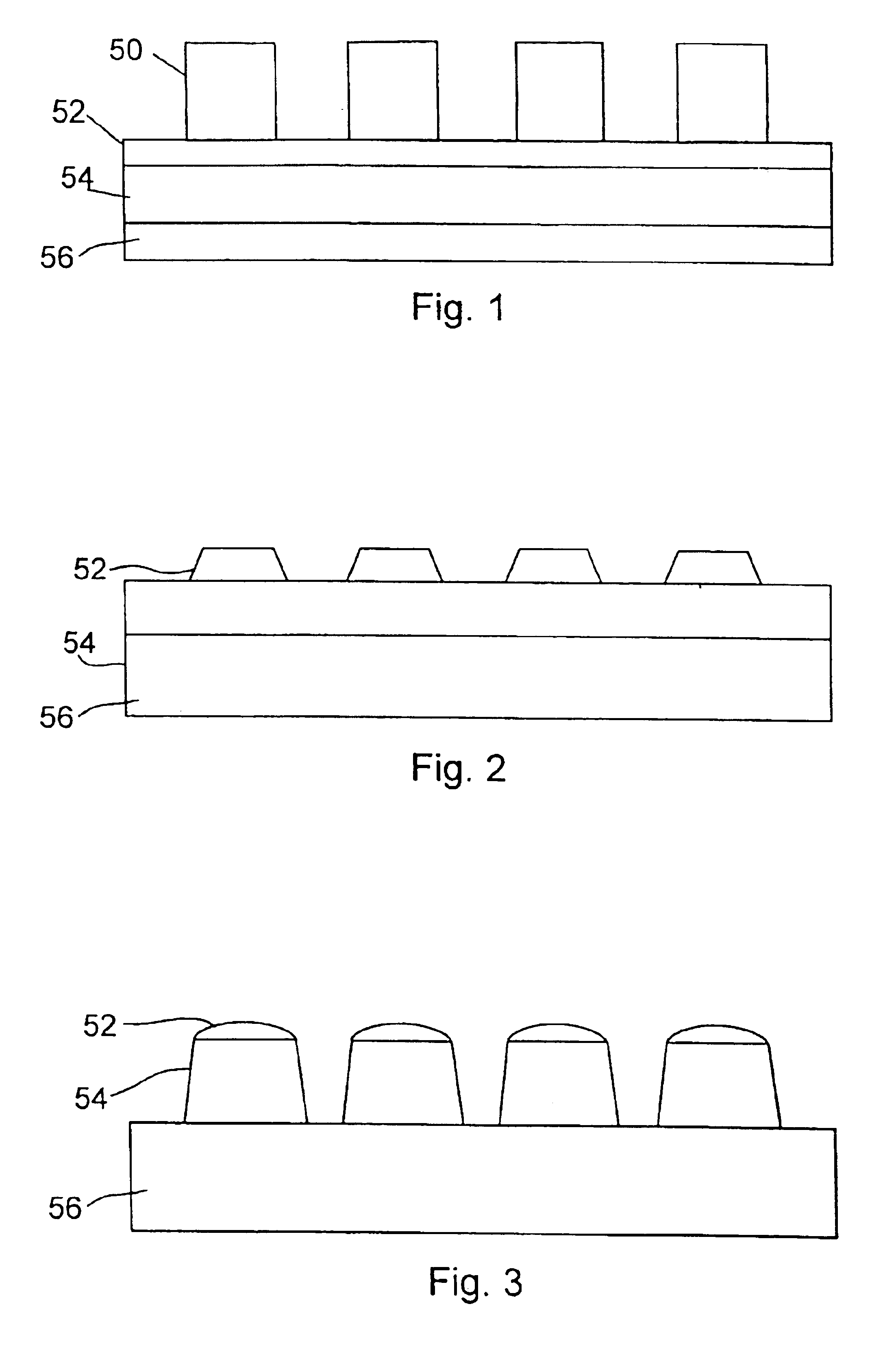
[0015]In another aspect of the invention, the method includes increasing the rate that one of an oxide, a nitride, a fluoride, a boride or a carbide forms on the hard mask in order to slow down the rate of erosion of the hard mask.
[0017]A further aspect of the present invention is to provide a method for containing critical dimension growth during an etching process including the step for placing a wafer or other substrate, for making by way of example only, a semiconductor product, a magnetic head or a flat panel display, with a hard mask disposed over a layer to be etched in a reactor, wherein the hard mask has at least one of a low sputter yield and a low reactivity to the etch chemistry of the etch process.
[0018]Accordingly, it is an object of the present invention to contain, control and minimize the growth of the critical dimension of a feature being etched.
[0019]It is still a further object of the present invention to perform the methodology of controlling and minimizing the critical dimension growth of a feature during an etch process, whether the process be conducted at low (below atmospheric) pressure, atmospheric pressure, or high (above atmospheric) pressure.

Problems solved by technology

Such growth of the critical dimension can disadvantageously diminish the space between the features and thereby adversely affect the functionality of the features.
However, such soft and hard masks have not been found to be particularly useful in controlling the critical dimension growth.

Method used


Image

  • Method for using a hard mask for critical dimension growth containment
  • Method for using a hard mask for critical dimension growth containment
  • Method for using a hard mask for critical dimension growth containment

Examples


Embodiment Construction

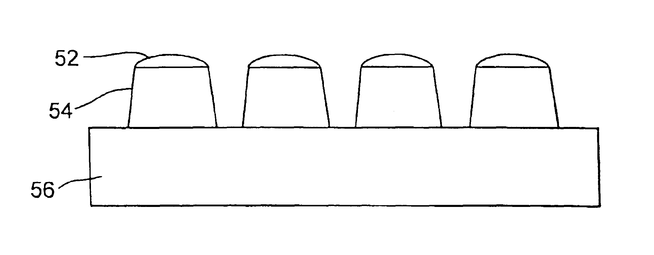
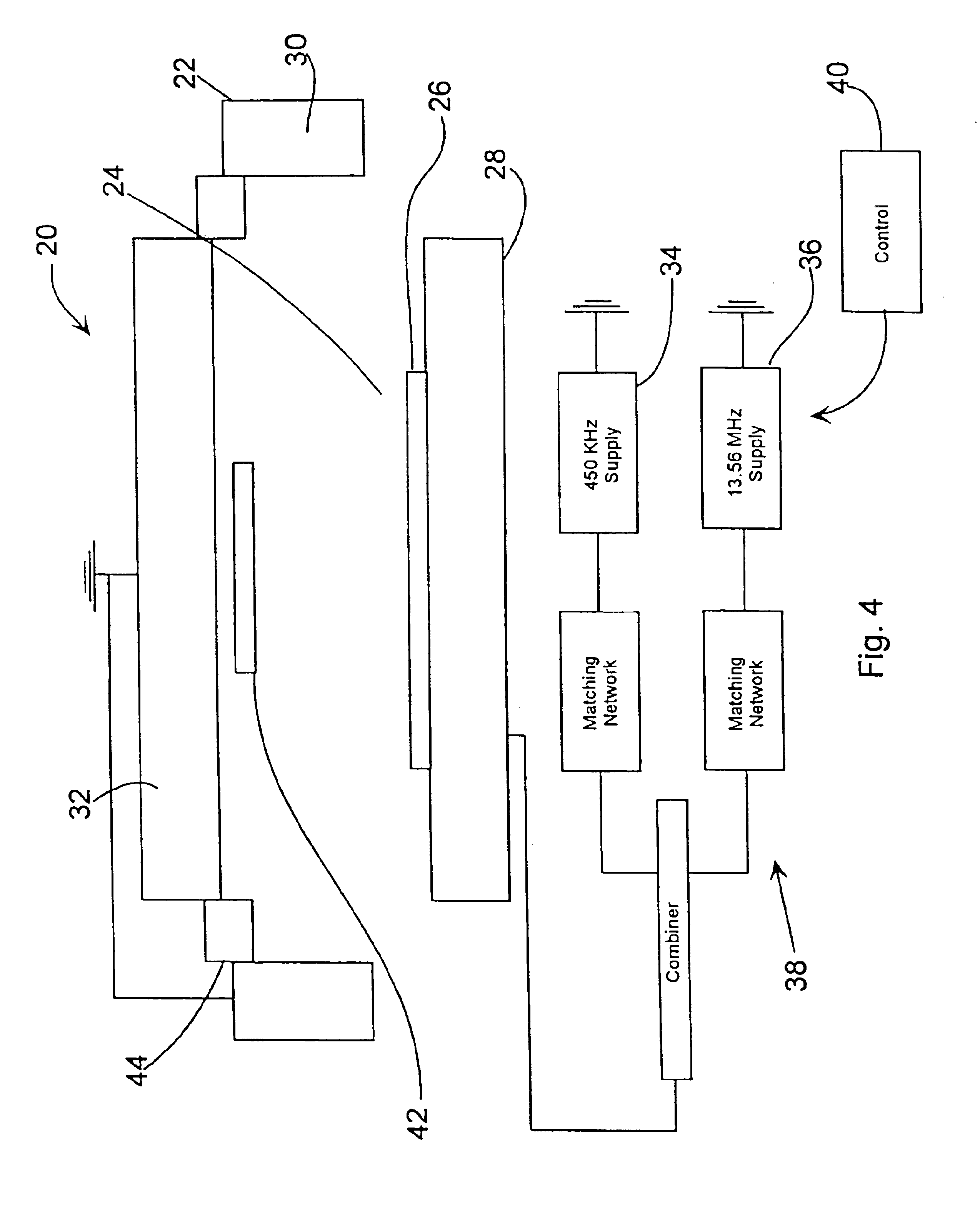
[0025]The method of the present invention can be performed in an etch reactor such as the etch reactor depicted in FIG. 4. It is to be understood that other reactors including but not limited to other etch reactors can be used and be within the spirit and scope of the invention.

[0026]The etch reactor of FIG. 4 is identified by the number 20 and is configured as a multi-frequency, tri-electrode reactor. The etching apparatus 20 includes a housing 22 and an etching chamber 24. A wafer 26 is positioned on a chuck incorporated into a bottom electrode 28. The chamber 24 further includes a side peripheral electrode 30 and an upper electrode 32. In a preferred embodiment, the side peripheral electrode 30 can be grounded or allowed to establish a floating potential as a result of the plasma developed in the chamber 24. The upper electrode 32 is generally grounded, but could also be designed to have a floating electrical potential. In typical operation, both the side peripheral electrode 30 ...


PUM


Abstract

A method for containing the critical dimension growth of the feature on a semiconductor substrate includes placing a substrate with a hard mask comprised of a reactive metal or an oxidized reactive metal in a chamber and etching the wafer. The method further includes using a hard mask which has a low sputter yield and a low reactivity to the etch chemistry of the process.

Description

[0001]This application is a continuation of Ser. No. 09 / 692,007 filed Oct. 19, 2000, which is a continuation of Ser. No. 09 / 009,369, filed Jan. 20, 1998, now U.S. Pat. No. 6,287,975.FIELD OF THE INVENTION[0002]The present invention is directed to a method for minimizing and containing the critical dimension growth of a feature on a semiconductor wafer and any other product, such as for example, the magnetic head for a disk drive and a flat panel display, which could be constructed using semiconductor processing techniques.BACKGROUND OF THE INVENTION[0003]The critical dimension (CD) of a feature on a semiconductor wafer, or any product fabricated using semiconductor processing techniques, is a width of that feature. The pitch is generally defined as a critical dimension plus the distance to the next feature.[0004]For semiconductor process methods using etch techniques, lithographic masking layers, such as for example photoresist layers, can be formed on top of the material to be etch...

Claims


Application Information

Patent Timeline
IPC IPC(8): H01L21/033H01L21/02H01L21/308H01L21/3213
CPCH01L21/0332H01L21/3081H01L21/32139
Inventor DEORNELLAS, STEPHEN P.JERDE, LESLIE G.COFER, ALFERD
Owner SPTS TECH LTD
Learn More