Method and apparatus for inspecting a semiconductor device

Active Publication Date: 2005-10-04
HITACHI HIGH-TECH CORP
View PDF6 Cites 50 Cited by
  • Summary
  • Abstract
  • Description
  • Claims
  • Application Information

AI Technical Summary

Benefits of technology

[0010]In addition, this invention makes it easier to determine the causes of failures by providing a function for displaying the time series data of inspection results for each piece of equipment which treated the wafer. In other words, this invention provides a method of inspecting a wafer, on the surface of which the same pattern is repetitively formed, which method comprises the steps of obtaining a charged particle beam image of a desired area of the wafer by detecting secondary charged particles

Problems solved by technology

In a semiconductor device, a conduction failure of contact holes leads to fatal defects, including characteristic failures, and has a significant impact on the yield of the semiconductor device.
Such a failure is often caused by changes in production requirements or defective operation of manufacturing equipment and often results in the production of a large amount of defective units.
However, the evaluation of pattern geometries alone cannot directly identify the conducting state of contact parts.
However, this method requires a considerably long tine to obtain an SEM image with a high signal-to-noise ratio and high resolution; in this regard, it takes a few hours to tens of hours to perform inspection of a whole wafer.
Therefore, th

Method used


Image

  • Method and apparatus for inspecting a semiconductor device
  • Method and apparatus for inspecting a semiconductor device
  • Method and apparatus for inspecting a semiconductor device

Examples


Example

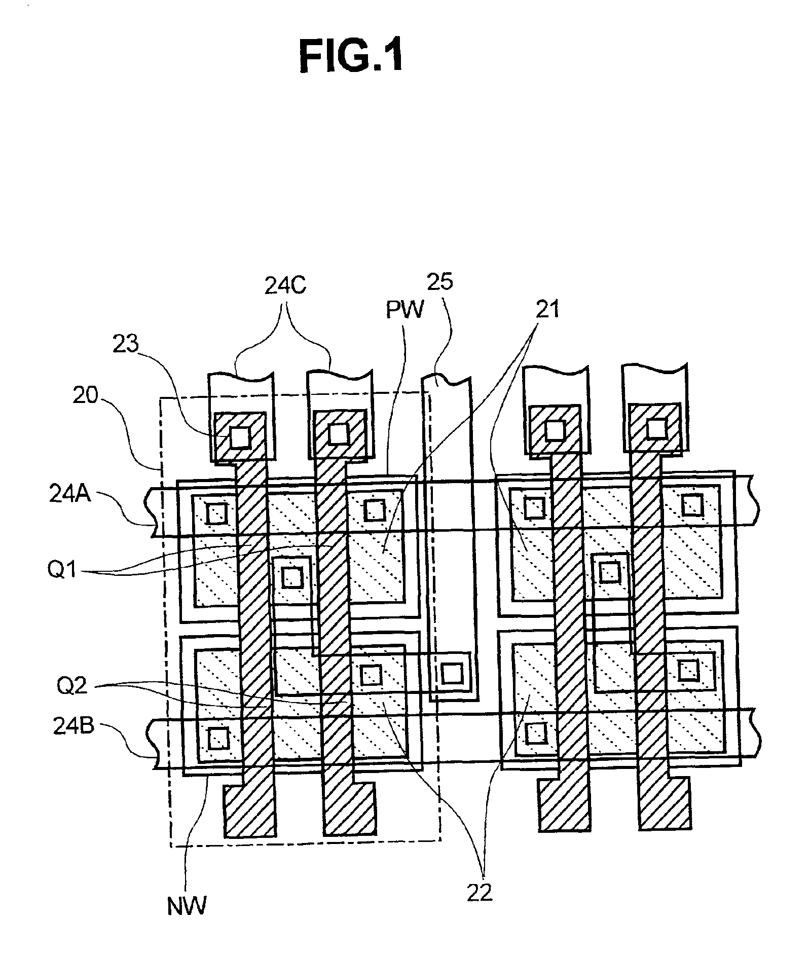
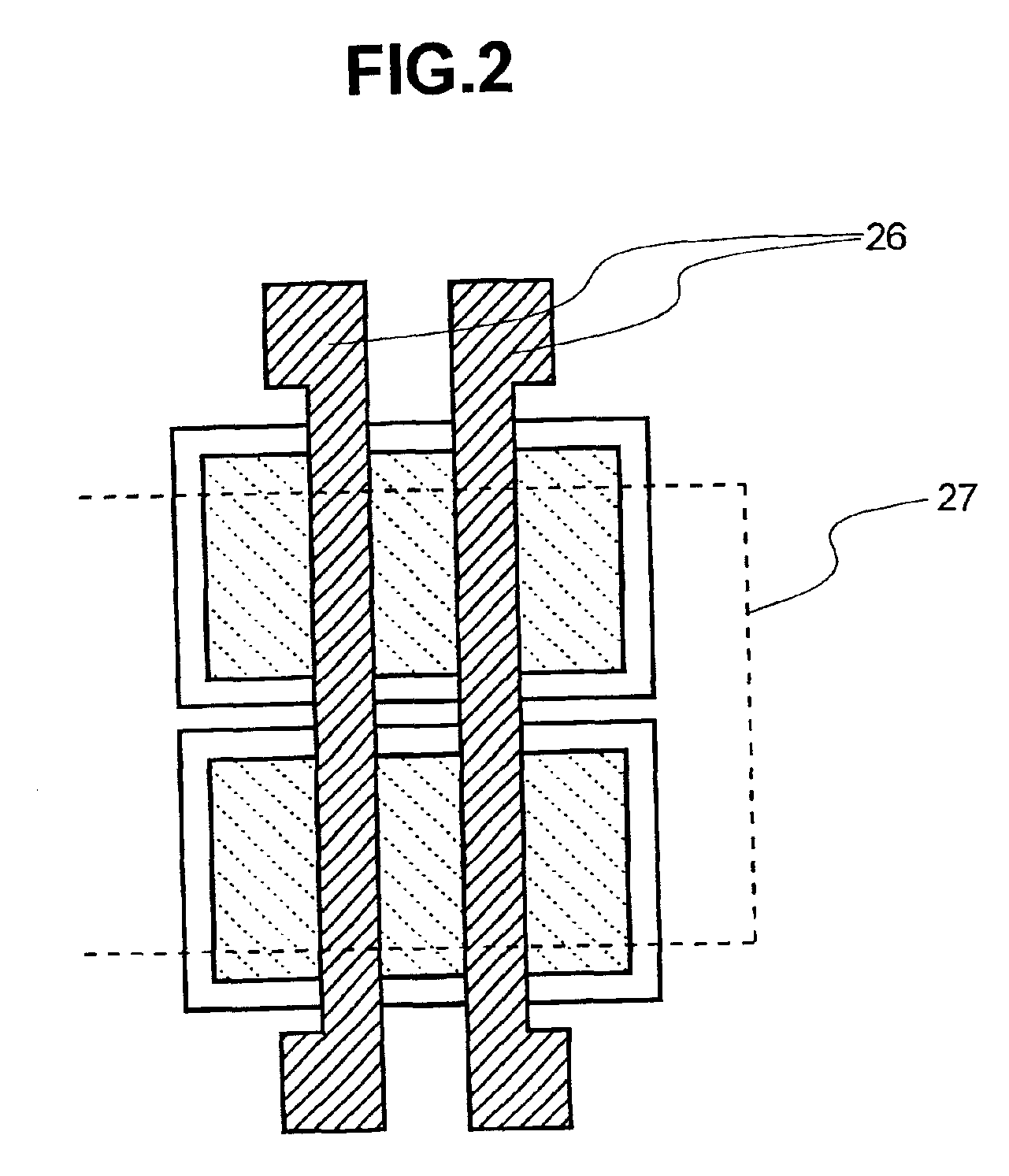
[0047]FIG. 1 shows an example of a logic unit of a semiconductor device, which is an object sample of the invention. This logic unit consists of a unit cell 20, which is enclosed with a phantom line in FIG. 1. The unit cell 20 consists of two n-channel MOS chips Q1 and two p-channel MOS chips Q2. The n-channel MOS chip Q1 is formed on an n-type region 21 in the surface of a p-WELL region PW formed on a substrate, and the p-channel MOS chip Q2 is formed on a p-type region 22 in the surface of an n-WELL region NM, respectively. Here, a plane view of a unit cell, before different types of traces 24A, 24B, 24C, and 25 are formed on it, is shown in FIG. 2. Reference numeral 26 denotes a polysilicon gate pattern. This unit cell is structured in such a way that 2-input NAND gates and 2-input NOR gate circuits can be formed efficiently by selecting traces to be subsequently added as necessary, and this structure is also extended to the structures connecting a large number of CMOS chips.

[004...


PUM


Abstract

A method and apparatus for inspecting a semiconductor device in which failure occurence conditions on a whole wafer are estimated by calculating the statistic of potential contrasts in pattern sections from sampled images to implement higher throughput, and defective conditions of a process are detected at an early stage with the help of time series data of the estimate result.

Description

BACKGROUND OF THE INVENTION[0001]This invention relates to technique for inspecting a semiconductor device; and, more particularly, the invention relates to a wafer inspection method and apparatus suitable for control of defective conditions which occur in the fabricating processes carried out in a semiconductor device production line.[0002]In a semiconductor device, a conduction failure of contact holes leads to fatal defects, including characteristic failures, and has a significant impact on the yield of the semiconductor device. Such a failure is often caused by changes in production requirements or defective operation of manufacturing equipment and often results in the production of a large amount of defective units. Such defective conditions in process are controlled, in general, by periodically checking for changes in pattern geometries with a critical dimension measurement SEM. However, the evaluation of pattern geometries alone cannot directly identify the conducting state o...

Claims


Application Information

Patent Timeline
IPC IPC(8): G01N23/225G01N23/22G01R31/302G01Q20/04G01Q30/04H01L21/027H01L21/66
CPCG01N23/2251
Inventor TANAKA, MAKIWATANABE, MASAHIROWATANABE, KENJINOZOE, MARIMIYAI, HIROSHI
Owner HITACHI HIGH-TECH CORP
Why Eureka
Try Eureka