Method of manufacturing semiconductor device

a manufacturing method and semiconductor technology, applied in the testing/measurement of individual semiconductor devices, semiconductor/solid-state devices, instruments, etc., can solve the problems of reducing the reliability of forming penetrating electrodes and reducing the yield of semiconductor devices, and achieve the effect of improving reliability

Active Publication Date: 2005-10-11
ADVANCED INTERCONNECT SYST LTD
View PDF16 Cites 51 Cited by
  • Summary
  • Abstract
  • Description
  • Claims
  • Application Information

AI Technical Summary

Benefits of technology

[0006]An exemplary embodiment of the invention addresses the above-mentioned and / or other problems, and enhances and / or improves reliability in a method of forming a semiconductor device.
[0007]An exemplary method of manufacturing a semiconductor device of the present invention includes (a) forming a conductive part within a concave portion that is formed in a first surface of a semiconductor substrate having an integrated circuit, (b) thinning the semiconductor substrate by removing a part of a second surface of the semiconductor substrate so as to make the conductive part penetrate from the first surface to the second surface, (c) cutting the semiconductor substrate into pieces. The method may also include inspecting an electric property of the semiconductor substrate through the conductive part following step (a). In accordance with the above-described exemplary method of manufacturing a semiconductor device, since an electric property of the semiconductor substrate is checked after the formation process of the conductive part, the inspection process does not adversely affect reliability in the formation process of the conductive part. Consequently, reliability of the method of manufacturing a semiconductor device will be enhanced and / or improved.
[0008]In the exemplary method of manufacturing a semiconductor device, the conductive part may be formed to have a brazing layer on its top surface in step (a). For example, the brazing layer is soft so that an end terminal of an inspection tool can securely contact with the conductive part without slipping. Even if a trace is marked on the top surface part of the conductive part when the end terminal contacted, the mark can be reduced or eliminated by melting at least a part of the brazing layer in a later process.
[0010]In the exemplary method of manufacturing a semiconductor device, the inspecting process may be conducted before step (b). This will make a handling of the semiconductor substrate easier compared to a case which the inspection process is carried out after the thinning process. In particular, it can prevent the semiconductor substrate from being impaired.
[0011]In the exemplary method of manufacturing a semiconductor device, step (c) may further include (c1) providing a reinforcing member on the semiconductor substrate, (c2) conducting the inspecting process and (c3) cutting the semiconductor substrate. As such, a handling of the semiconductor substrate may be easier since the semiconductor substrate is reinforced with the reinforcing member. In particular, it may prevent the semiconductor substrate from being impaired.

Problems solved by technology

This decreases reliability in forming the penetrating electrode, and it can lead to a lower yield of the semiconductor device.

Method used


Image

  • Method of manufacturing semiconductor device
  • Method of manufacturing semiconductor device
  • Method of manufacturing semiconductor device

Examples


Embodiment Construction

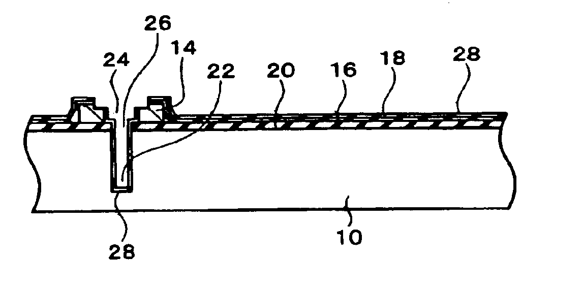
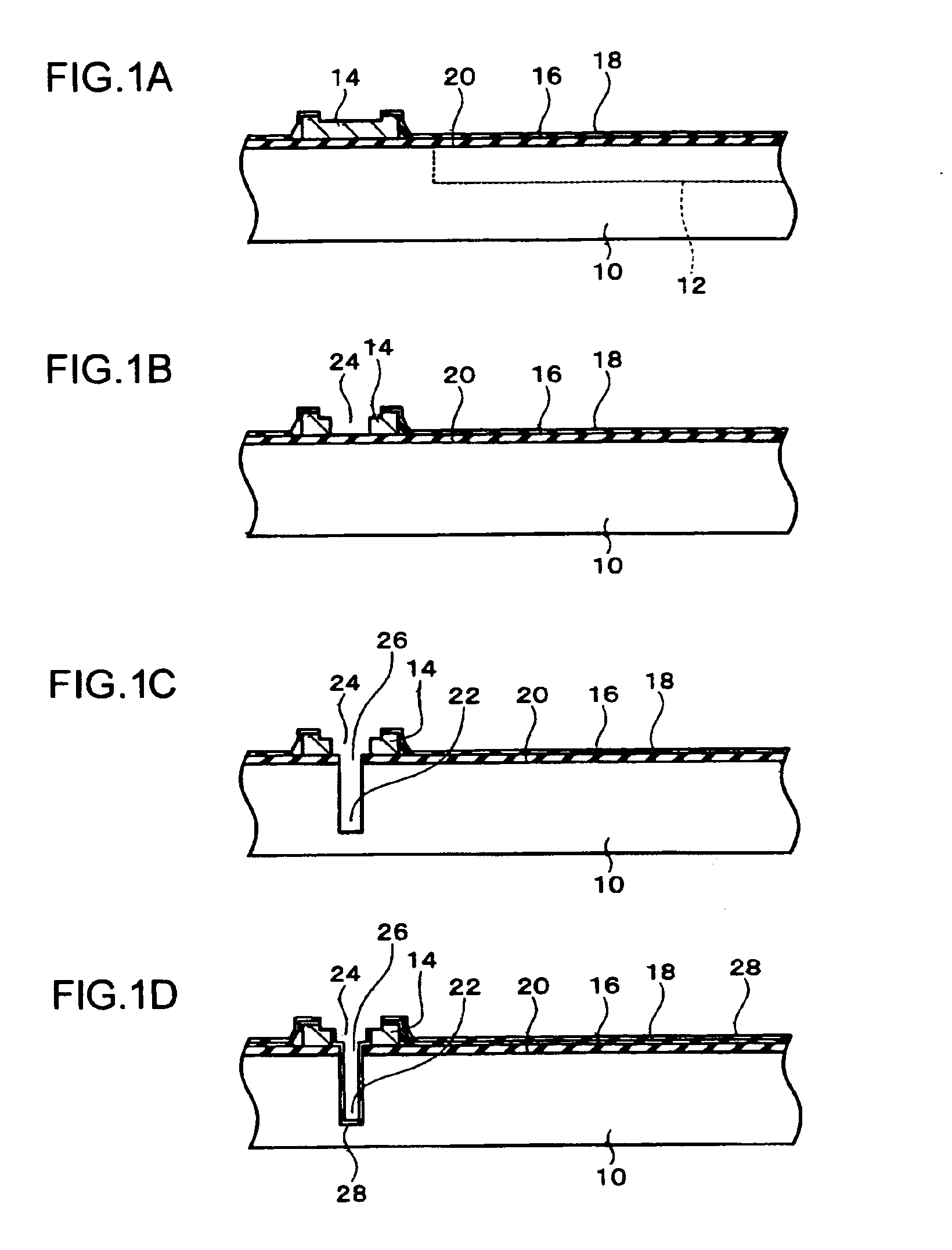
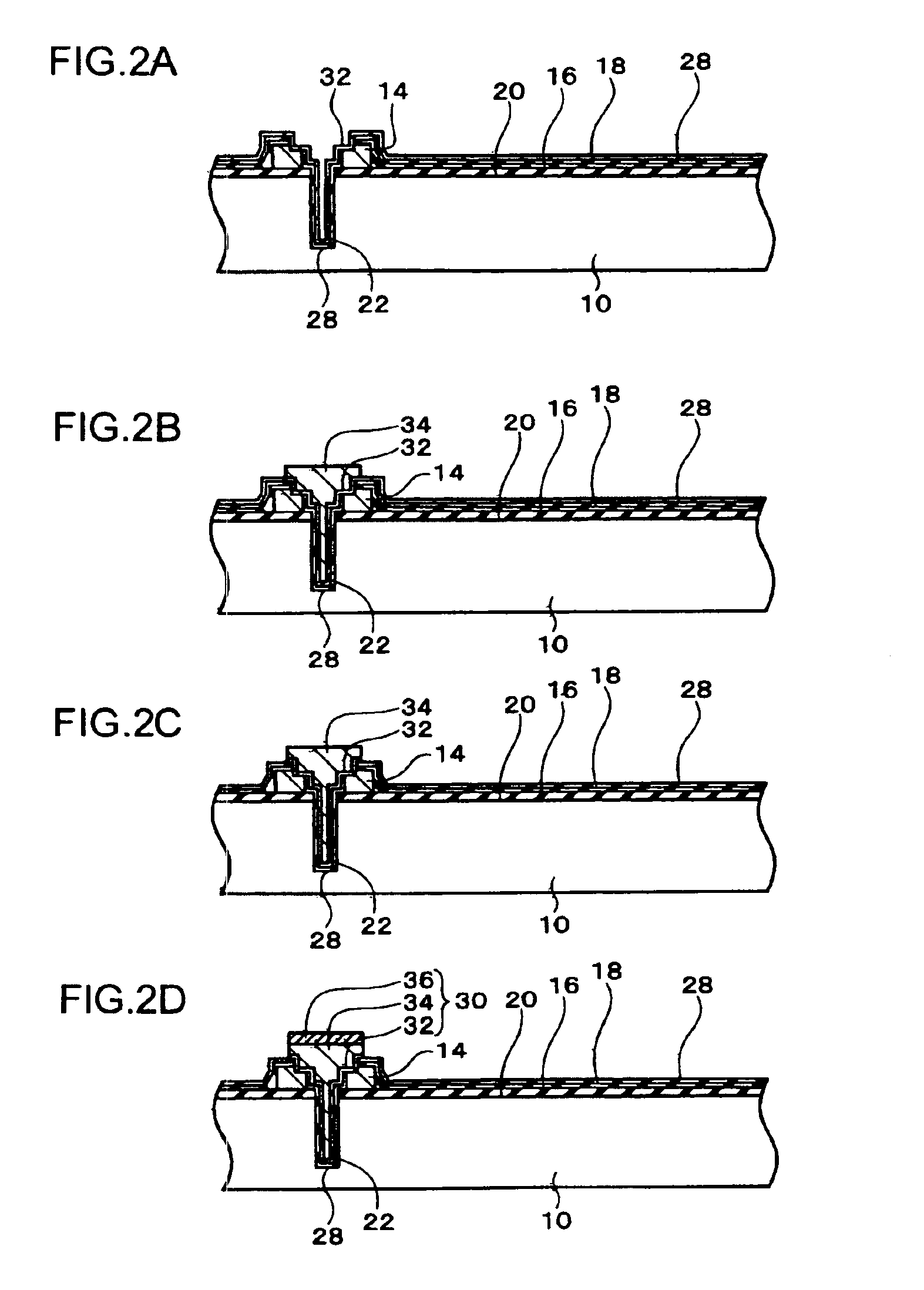
[0019]Exemplary of the present invention are described below with reference to the accompanying figures. FIG. 1A through FIG. 4 show a method of manufacturing a semiconductor device according to an exemplary embodiment of the present invention.

[0020]A semiconductor substrate 10 (for example, a silicon substrate) is provided. The semiconductor substrate 10 may be a semiconductor wafer or a semiconductor chip. On the semiconductor substrate 10, an integrated circuit 12 is formed. In a case of the semiconductor wafer, the integrated circuit 12 is provided in the plural number (see FIG. 3A). In a case of the semiconductor wafer, a single of the integrated circuit 12 is formed. An electrode 14 (for example, a pad) electrically coupled with the integrated circuit 12 is formed on the semiconductor substrate 10. The electrode 14 is provided in the plural number to each integrated circuit 12. The electrode 14 of provided in the plural number may be arranged along edges of the integrated circ...


PUM


Abstract

To enhance and / or improve reliability in a method of forming a semiconductor device. An exemplary method of forming a semiconductor device forms a conductive part within a concave portion which is formed in a first surface of a semiconductor substrate. The semiconductor substrate includes an integrated circuit. The method also thins the substrate by removing a part of a second surface of the semiconductor substrate so as to make the conductive part penetrate from the first surface to the second surface, and cuts the semiconductor substrate into pieces. An electric property of the semiconductor substrate is inspected through the conductive part after the conductive part is formed.

Description

BACKGROUND OF THE INVENTION[0001]1. Field of Invention[0002]The present invention relates to a method of manufacturing a semiconductor device.[0003]2. Description of Related Art[0004]The related are includes a semiconductor device with three-dimensional mounting. Also, in accordance with the related art, a penetrating electrode is formed on a semiconductor substrate, and more than one semiconductor substrate is stacked-up, and then the penetrating electrode formed on a upper substrate and the penetrating electrode formed on a lower substrate are coupled. In a related art method, an inspection process checking an electric property of the semiconductor substrate is conducted before the penetrating electrode is formed. In the inspection process, since an end terminal of an inspection tool contacts with the electrode (an aluminum pad), a trace sometimes remains on the surface of the electrode. This decreases reliability in forming the penetrating electrode, and it can lead to a lower yi...

Claims


Application Information

Patent Timeline
Patent Type & Authority Patents(United States)
IPC IPC(8): H01L21/66H01L25/065H01L21/301H01L21/304H01L21/3205H01L21/78H01L23/52H01L25/07H01L25/18
CPCH01L21/78H01L22/20H01L21/304H01L25/0657H01L2224/16145H01L2225/06513H01L2225/06541H01L2225/06596H01L2924/014H01L21/76898H01L24/05H01L2224/02377H01L2224/05001H01L2224/05009H01L2224/05124H01L2224/05147H01L2224/13025H01L2924/00014
Inventor YAMAGUCHI, KOJI
Owner ADVANCED INTERCONNECT SYST LTD
Why Eureka
Try Eureka