Organic EL circuit

a technology of organic el and circuits, applied in the field of organic el circuits, can solve problems such as uneven display, and achieve the effects of finer gray scale control, removing the threshold voltage of driving transistors, and facilitating gray scale control

Inactive Publication Date: 2005-10-11
SANYO ELECTRIC CO LTD
View PDF8 Cites 7 Cited by
  • Summary
  • Abstract
  • Description
  • Claims
  • Application Information

AI Technical Summary

Benefits of technology

[0010]The present invention was conceived to address the above mentioned problem, and one object of the present invention is to provide an organic EL circuit which can perform desirable gray scale control such that display unevenness is not generated.
[0011]In order to achieve at least the object mentioned above, according to the present invention, a plurality of organic EL elements (sub-pixels) are provided in a pixel, the plurality of organic EL elements are switched on and off, and driving transistors of different size are provided. With such a structure, the gray scale can be controlled by switching the driving transistors fully on. Therefore, the effect of the threshold voltage of the driving transistor can be removed and a preferable gray scale control can be achieved.
[0012]According to another aspect of the present invention, the size of each of the driving transistors is varied in order to vary the amount of light emission by the EL element. With such structure, the gray scale can be controlled by switching appropriate driving transistors fully on. In this manner, the effect of the threshold voltage of the driving transistor can be removed.
[0013]According to another aspect of the present invention, it is possible to perform a finer gray scale control by incorporating time division light emission.

Problems solved by technology

However, because there is an intrinsic difference in the threshold voltage (Vth) of the driving TFT2 for each pixel, the display of each pixel will not be equal, and, thus, the display will be uneven.

Method used


Image

  • Organic EL circuit
  • Organic EL circuit
  • Organic EL circuit

Examples


Embodiment Construction

[0020]A preferred embodiment of the present invention will now be described referring to the figures.

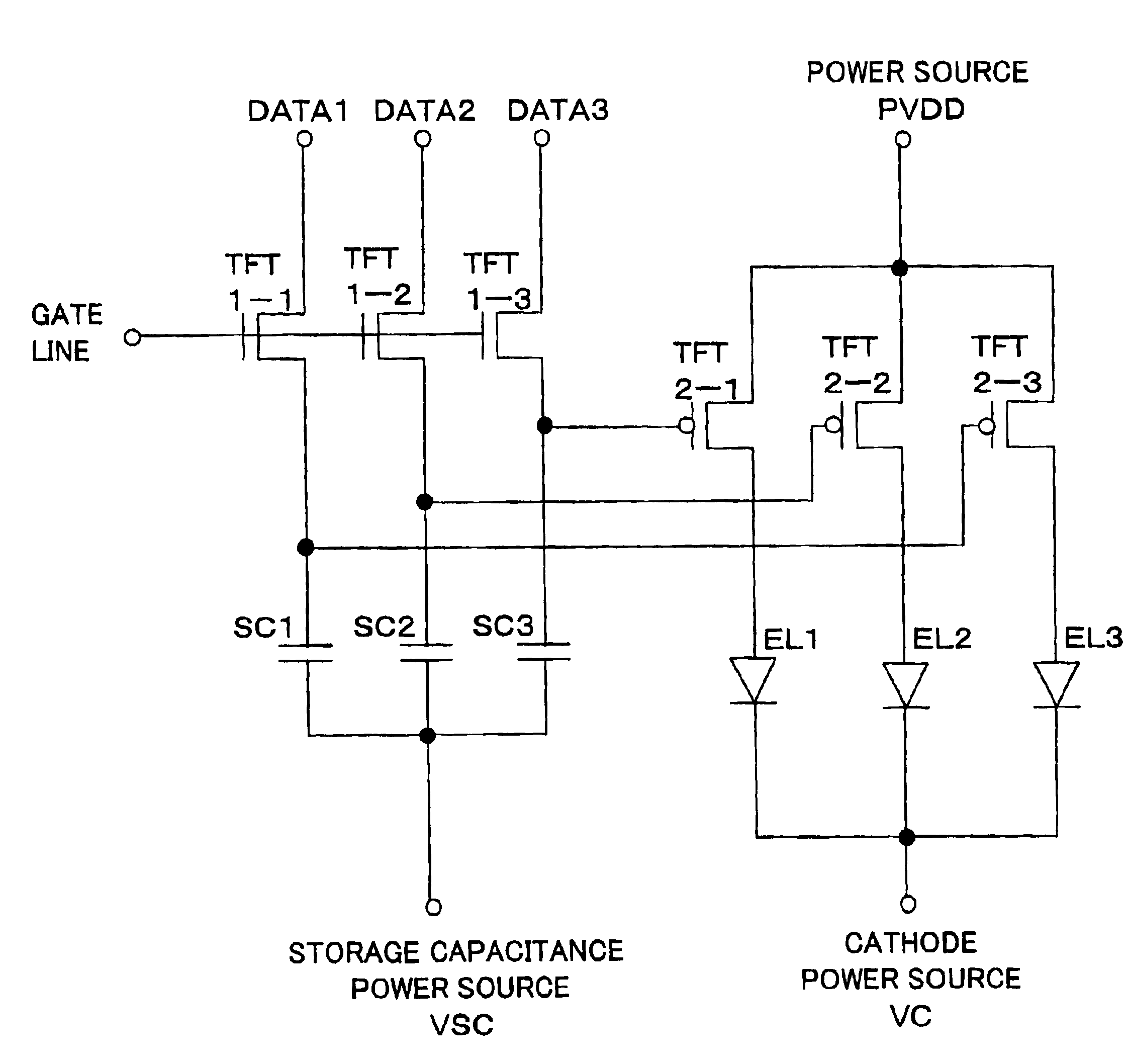
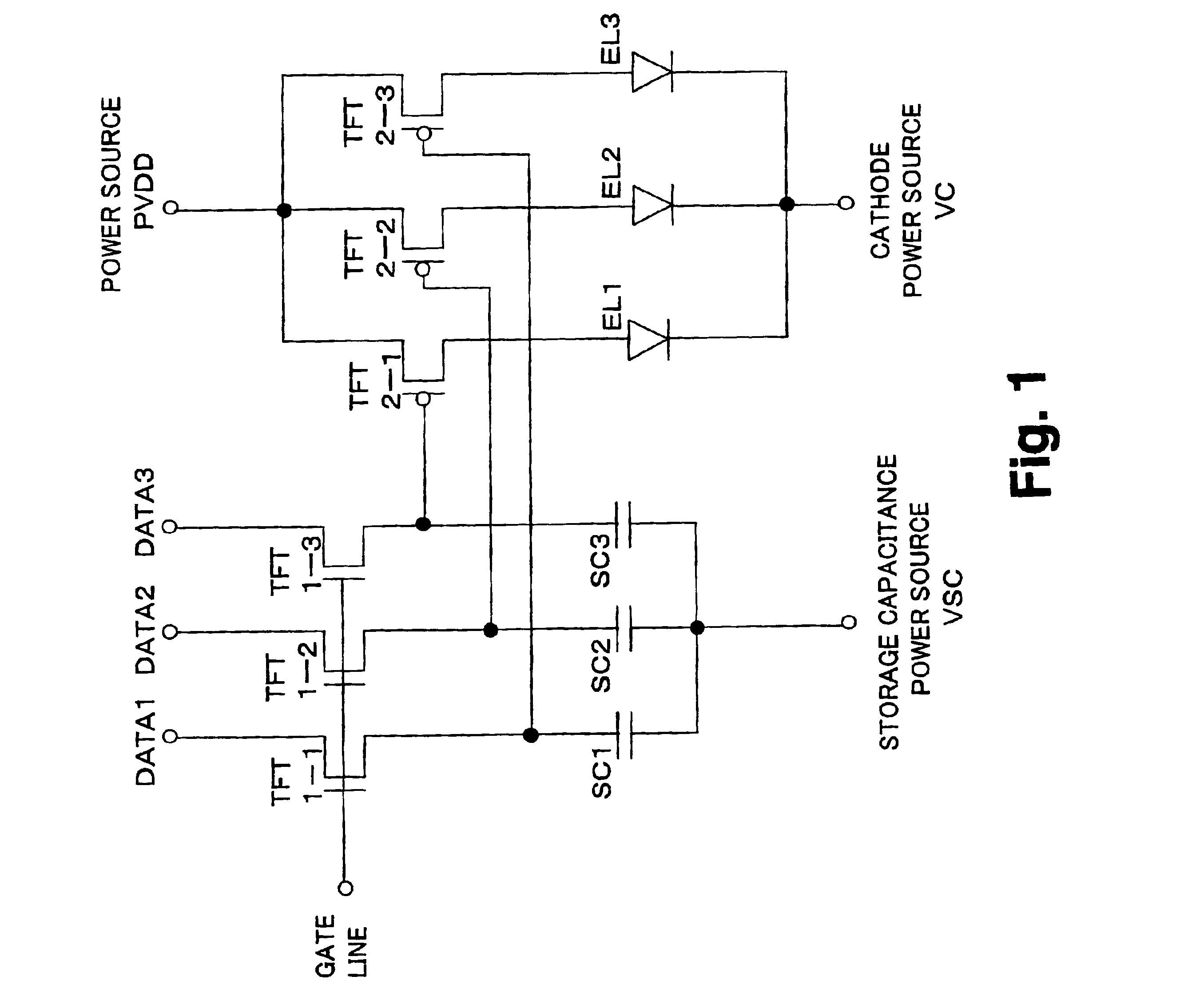
[0021]FIG. 1 is a diagram showing one pixel according to the preferred embodiment of the present invention. The gate line in the horizontal direction is connected to the gates of three n channel scan TFTs 1-1, 1-2, and 1-3. The three scan TFTs 1-1, 1-2, and 1-3 are simultaneously switched on for the duration of one horizontal period when the horizontal line is selected.

[0022]The drain of each of the scan TFTs 1-1, 1-2, and 1-3 is respectively connected to a separate data line DATA1, DATA2, and DATA 3. The source of each of the scan TFTs 1-1, 1-2, and 1-3, on the other hand, is respectively connected to a separate storage capacitor SC1, SC2, and SC3. The other terminal of each of the storage capacitors SC1, SC2, and SC3 is connected to a storage capacitance power source line VSC which is a power source line.

[0023]The connecting points between the sources of scan TFTs 1-1, 1-2, and 1-3...


PUM


Abstract

Using scan (TFT 1-1˜TFT 1-3) data having a size of 3 bits from data lines (DATA1˜DATA3) is stored in storage capacitors (SC1˜SC3). Driving TFTs (TFT 2-1˜TFT 2-3) are switched fully on by the voltage of these storage capacitors (SC1˜SC3). The on / off conditions of the driving TFTs (TFT 2-1˜TFT 2-3) are controlled according to digital data, to control the on / off conditions of organic EL elements (EL1˜EL3) and provide brightness control.

Description

BACKGROUND OF THE INVENTION[0001]1. Field of the Invention[0002]The present invention relates to an organic EL circuit including, corresponding to each of a plurality of pixels, a plurality of driving transistors switched on and off in accordance data from a plurality of data lines and a plurality of EL elements corresponding to the plurality of driving transistors.[0003]2. Description of the Related Art[0004]Conventionally, use of an organic EL panel as a flat panel display is known. Because each pixel in an organic EL panel is self-emitting, an organic EL panel has advantages including that, unlike a liquid crystal display, no backlight is required and that the display is relatively bright.[0005]FIG. 6 shows a structural example of a pixel circuit in a conventional organic El panel employing a thin film transistor (TFT). An organic EL panel is constructed by arranging elements such as these in a matrix form.[0006]A gate line which extends in the row direction is connected to the g...

Claims


Application Information

Patent Timeline
Patent Type & Authority Patents(United States)
IPC IPC(8): G09G3/38G09G3/20G09G3/32G09G3/30G09F9/30G09G3/34H05B33/02H05B33/14H05B33/00H05B33/08H05B44/00H01L27/32H01L51/50
CPCG09G3/2074G09G3/2081G09G3/3258G09G3/2022G09G3/2077G09G2300/0809G09G2300/0828G09G2300/0842G09G2300/0852G09G3/30
Inventor KOMIYA, NAOAKI
Owner SANYO ELECTRIC CO LTD
Why Eureka
Try Eureka