Method and apparatus for gas temperature control in a semiconductor processing system

a technology of semiconductor processing and gas temperature control, which is applied in the direction of lighting and heating apparatus, indirect heat exchangers, machine operation modes, etc., can solve the problems of reducing the likelihood of gas phase reaction of reactants, and affecting the efficiency of gas phase reaction

Inactive Publication Date: 2005-10-18
APPLIED MATERIALS INC
View PDF172 Cites 75 Cited by
  • Summary
  • Abstract
  • Description
  • Claims
  • Application Information

AI Technical Summary

Benefits of technology

[0009]One aspect of the present invention generally provides a gas temperature control apparatus for controlling the temperature of process gases flowing into a processing chamber. In one embodiment, a gas temperature control apparatus for se

Problems solved by technology

Many traditional deposition processes have difficulty filling sub-micron structures where the aspect ratio exceeds 4:1, and particularly where the aspect ratio exceeds 10:1.
Therefore, there is a great amount of ongoing effort being directed at the formation of substantially void-free and seam-free sub-micron features having high aspect ratios.
A pulse of a purge gas and/or a pump evacuat

Method used


Image

  • Method and apparatus for gas temperature control in a semiconductor processing system
  • Method and apparatus for gas temperature control in a semiconductor processing system
  • Method and apparatus for gas temperature control in a semiconductor processing system

Examples


Embodiment Construction

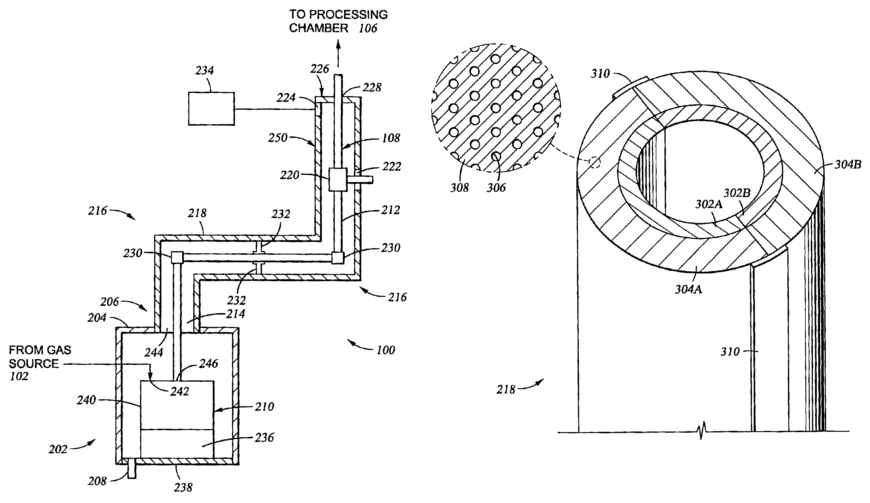
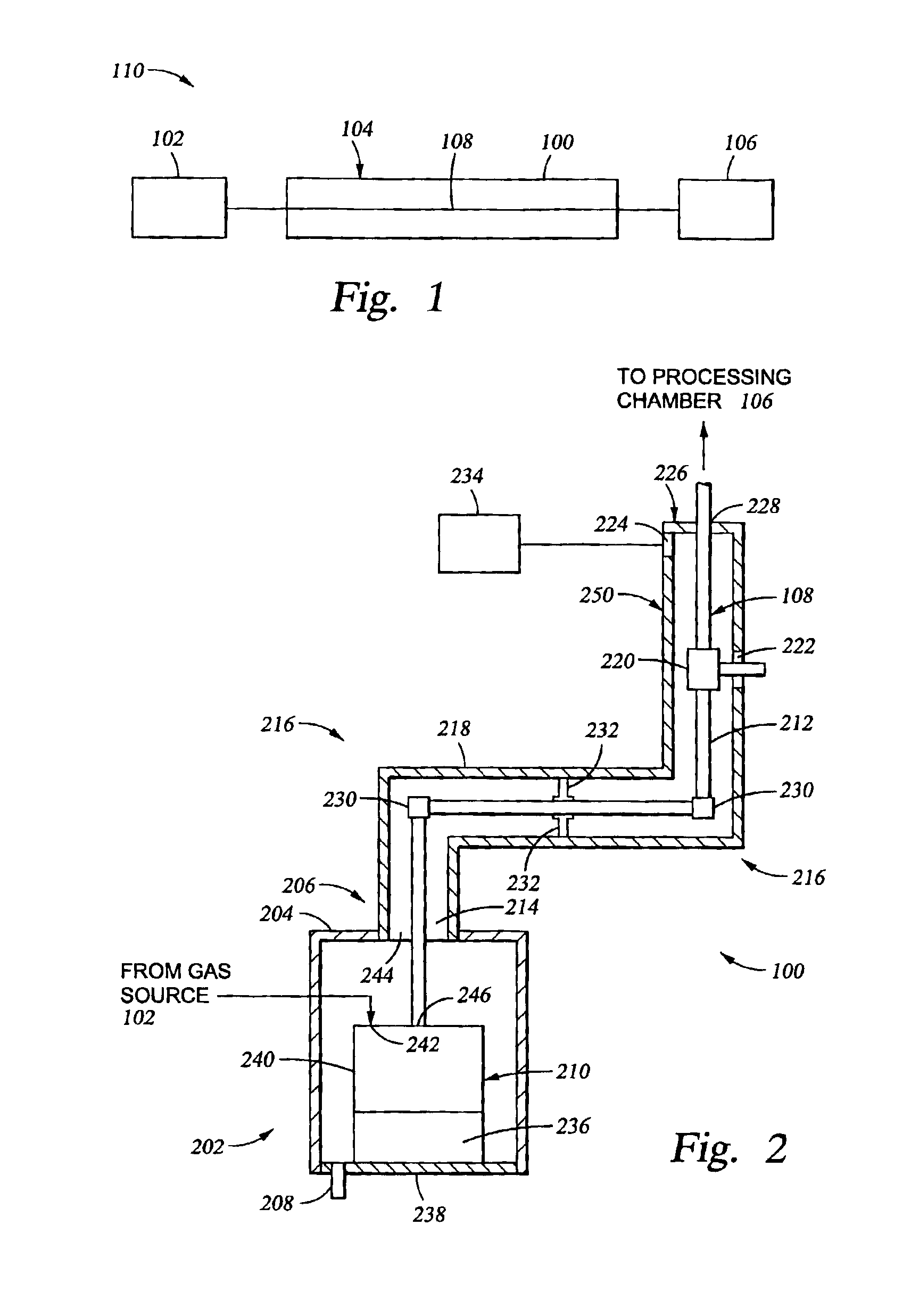
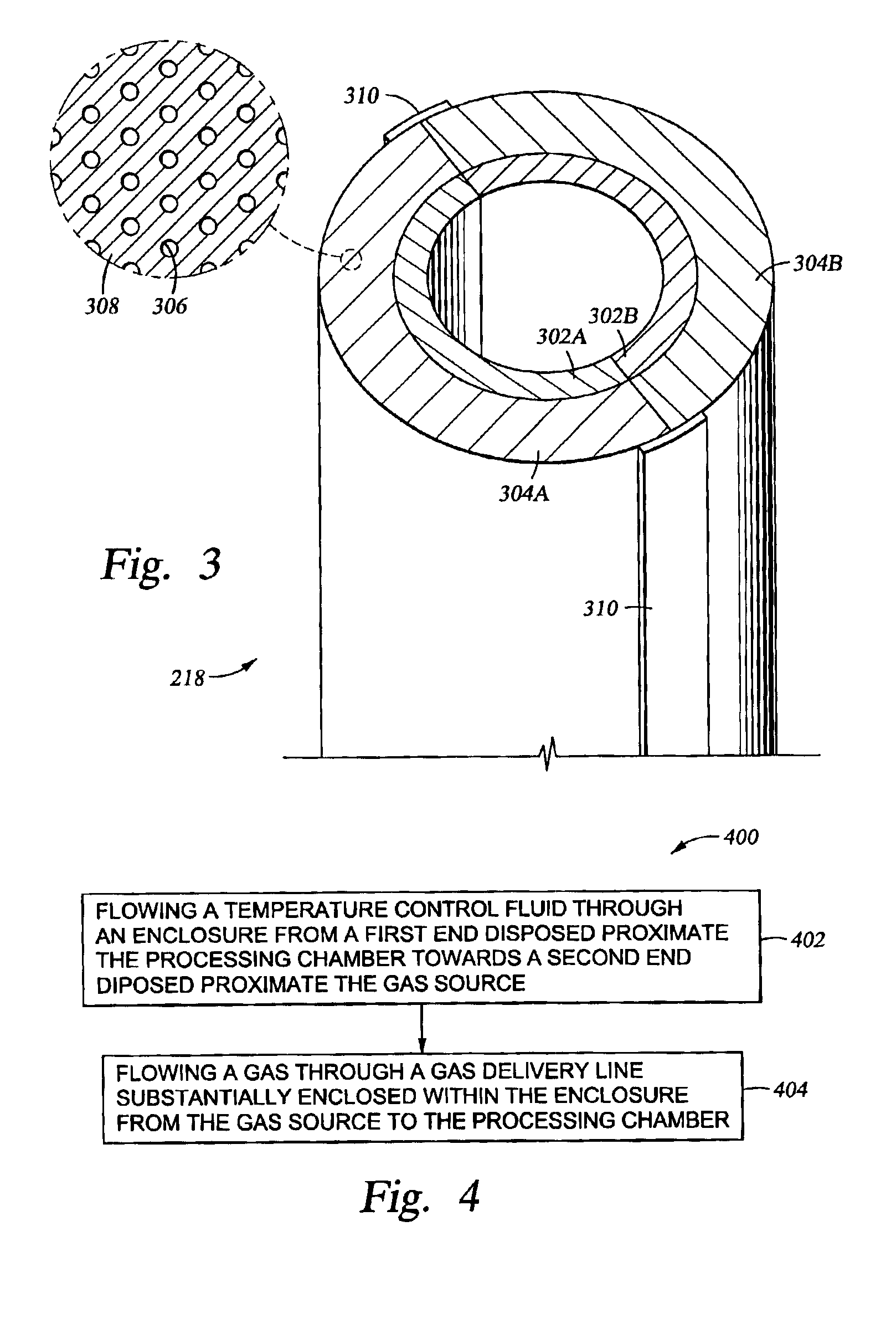
[0017]FIG. 1 is a simplified schematic of a processing system 110 having a gas delivery system 104 connecting a gas source 102 to a processing chamber 106. The gas delivery system 104 includes at least one gas delivery line 108 coupled between the gas source 102 and the processing chamber 106 and a gas temperature control apparatus 100 for controlling the temperature of at least one gas delivered via the gas delivery line 108 to the processing chamber 106.

[0018]The gas source 102 may be a single or multiple source coupled to the gas delivery system 104. The gas source 102 may be a local or remote vessel, a centralized facility source that supplies the gas throughout the facility, or any other suitable source of gas to be delivered to the processing chamber 106. The temperature controlled gases delivered to the processing chamber 106 may be a process gas, purge gas, cleaning gas, or other gas.

[0019]The processing chamber 106 is typically adapted for use in atomic layer deposition but...


PUM


Abstract

A method and apparatus for controlling the temperature of at least one gas flowing into a processing chamber is provided. In one embodiment, a gas temperature control apparatus for semiconductor processing includes a gas delivery line coupled between a processing chamber and a gas source. An enclosure substantially encloses the gas delivery line and is adapted to flow a heat transfer fluid away from the processing chamber.

Description

BACKGROUND OF THE INVENTION[0001]1. Field of the Invention[0002]Embodiments of the present invention generally relate to a method and apparatus for gas temperature control in a semiconductor processing system.[0003]2. Description of the Related Art[0004]Reliably producing sub-micron and smaller features is one of the key technologies for the next generation of very large scale integration (VLSI) and ultra large scale integration (ULSI) of semiconductor devices. However, as circuit technology continues to evolve, the shrinking dimensions of interconnects in VLSI and ULSI technology have placed growing demands for improved processing capabilities. The multilevel interconnects that lie at the heart of this technology require precise processing of high aspect ratio features, such as vias and other interconnects. Reliable formation of these interconnects is very important to VLSI and ULSI success and to the continued effort to increase circuit density and quality of individual substrates...

Claims


Application Information

Patent Timeline
IPC IPC(8): F28D7/10H01L21/00
CPCF28D7/106H01L21/67282F28F2270/00
Inventor KU, VINCENT W.CHEN, LINGWU, DIEN-YEHOUYE, ALAN H.WYSOK, IRENA
Owner APPLIED MATERIALS INC
Why Eureka
Try Eureka