Semiconductor device having multi-layer oxygen barrier pattern

a technology of oxygen barrier and semiconductor device, which is applied in the direction of semiconductor devices, capacitors, electrical equipment, etc., can solve the problems of deterioration of semiconductor devices, platinum electrodes that do not stop oxygen from entering the cell, and normal cell operation is not achieved, so as to prevent unwanted reactions

Inactive Publication Date: 2005-10-18
SAMSUNG ELECTRONICS CO LTD
View PDF4 Cites 7 Cited by
  • Summary
  • Abstract
  • Description
  • Claims
  • Application Information

AI Technical Summary

Benefits of technology

[0014]It is desirable that the oxygen barrier metal layer is comprised of iridium, and that an iridium oxide layer is formed between the oxygen barrier metal layer and a capacitor electrode. When the ferroelectric film is annealed at an oxygen environment, the iridium oxide layer can provide oxygen to the ferroelectric film, and at the same time can prevent unwanted reactions between the barrier layer and capacitor electrode. The ferroelectric film is typically formed by PZT(PbZrTiO3), BST(BaSrTiO3), BSTN, BSTT, etc.

Problems solved by technology

The more a semiconductor device is integrated, the more a size of capacitor is forced to be narrow, and thereby deterioration may occur in a semiconductor device.
However, the platinum electrode does not stop oxygen from penetrating.
The nonconductive silicon and tungsten (W) oxide film causes a high contact resistance, and thereby a normal operation of the cell is not achieved even when only a part of the surface or boundary surface is oxidized.
However, even though a very small amount of oxygen may enter into the barrier layer, the oxygen that penetrates the barrier layer forms an oxide film in a boundary surface of the contact plug connected with the barrier layer, and thereby contact resistance may be increased and a cell may not operate normally.
Namely, it creates problems by increasing the required driving voltage and operating time.

Method used


Image

  • Semiconductor device having multi-layer oxygen barrier pattern
  • Semiconductor device having multi-layer oxygen barrier pattern
  • Semiconductor device having multi-layer oxygen barrier pattern

Examples


Embodiment Construction

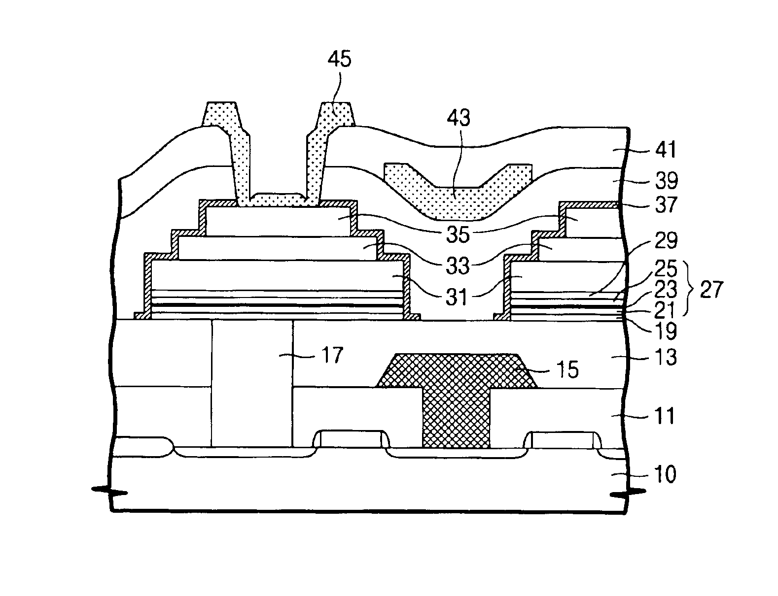
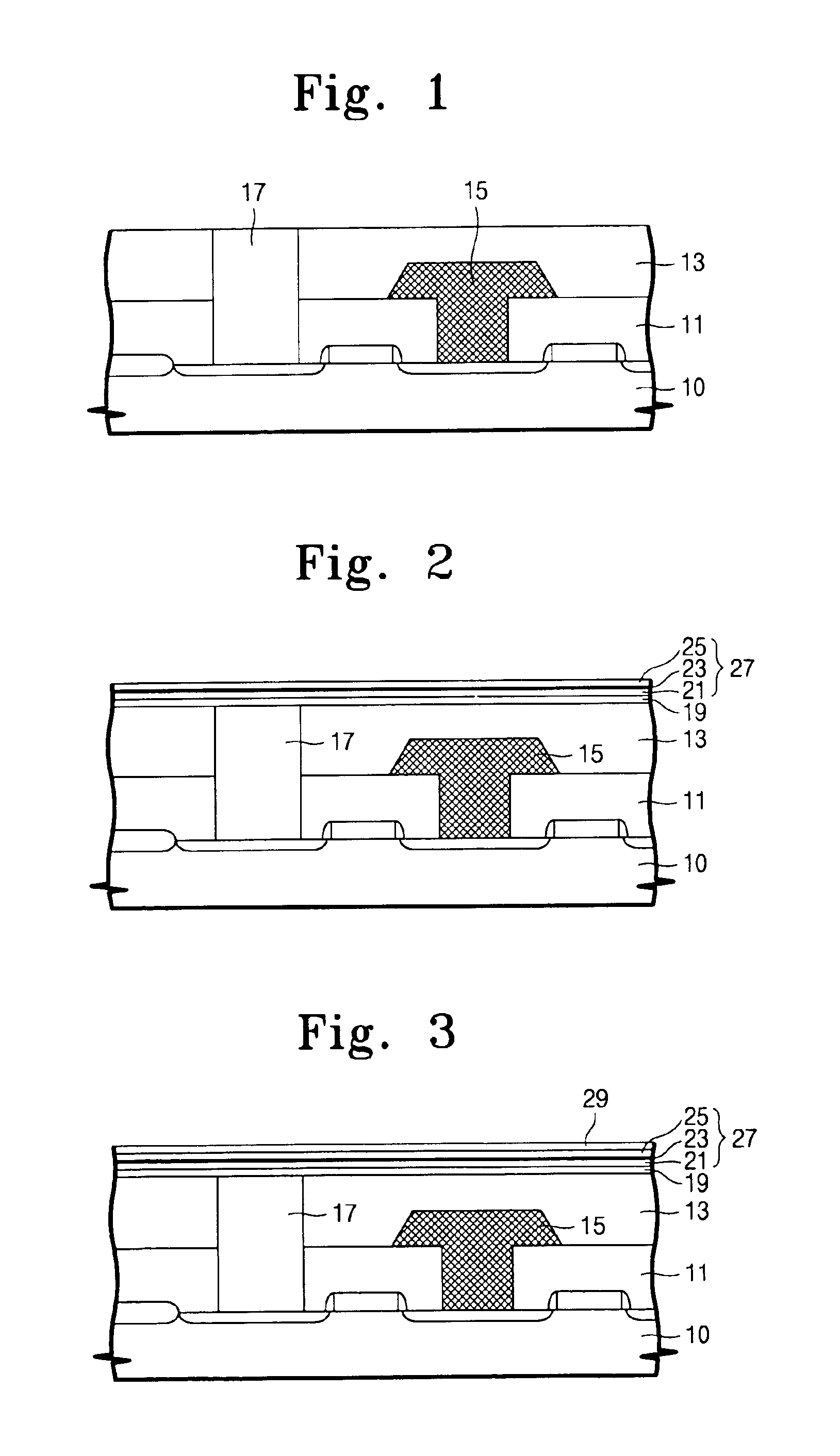
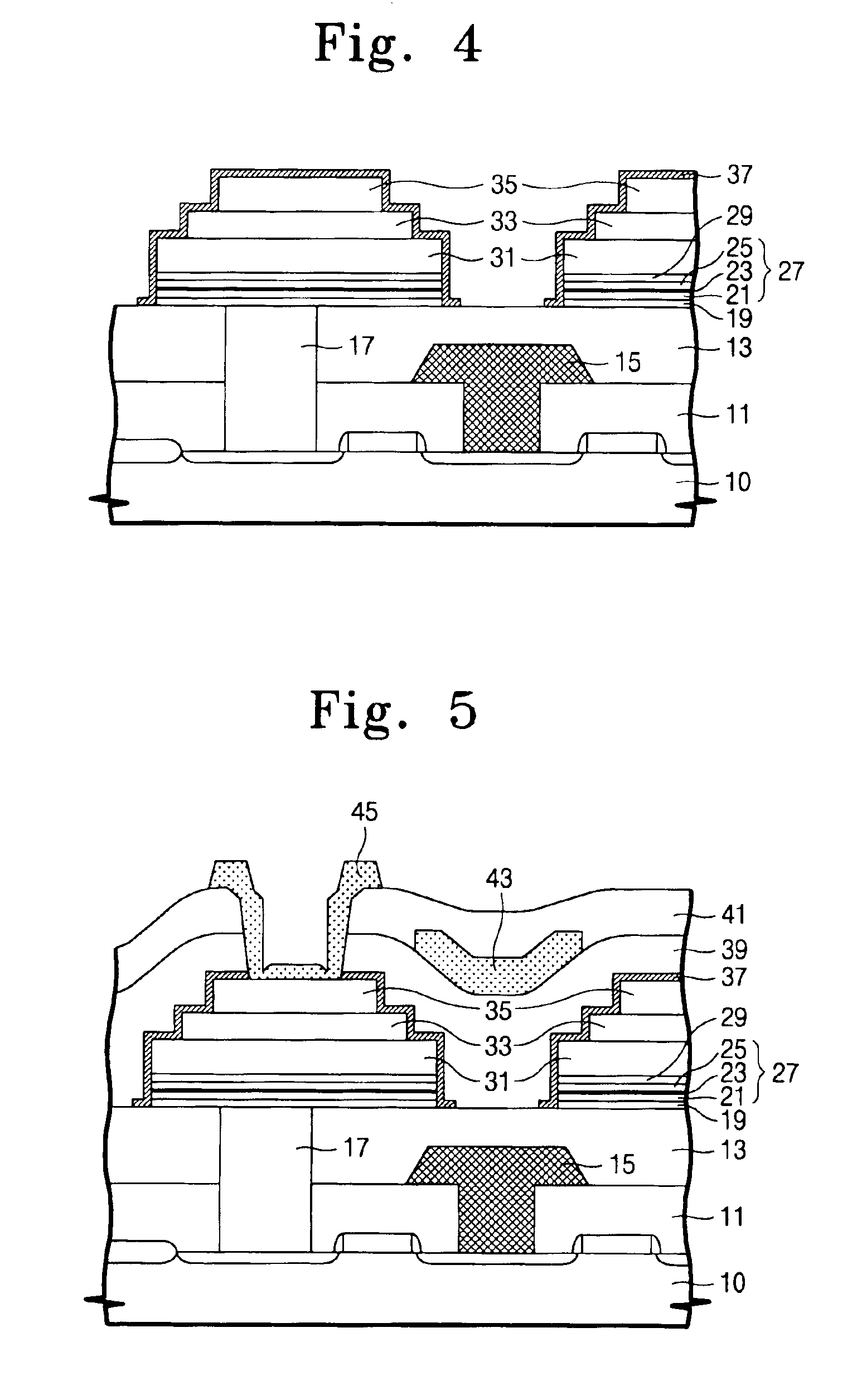
[0022]Referring to FIGS. 1 to 7, a preferred embodiment of the present invention will be described below.

[0023]FIGS. 1 to 5 are cross sectional diagrams illustrating the steps for forming a FRAM (Ferroelectric Random Access Memory device) in accordance with the present invention.

[0024]Referring to FIG. 1, field isolation (field-oxidation) is formed in a substrate 10, and MOS transistor structure having a gate, source and drain is constructed on the substrate 10. A first interlayer dielectric 11 is formed over the substrate 10 and the MOS transistor structure. After patterning the first interlayer dielectric 11 to form a bit line contact hole, a contact plug filling the bit line contact hole and bit line 15 connected to the contact plug are formed by stacking and patterning a first conductive film. A second interlayer dielectric 13 is formed on the bit line 15. A storage node contact hole is formed in the first and second interlayer dielectrics 13 and 15 by patterning, and the contac...


PUM

PropertyMeasurementUnit
driving voltageaaaaaaaaaa
temperatureaaaaaaaaaa
sizeaaaaaaaaaa

Abstract

The present invention relates to the field of a semiconductor device having a ferroelectric material capacitor and method of making the same. The semiconductor device includes a capacitor having a triple-level oxygen barrier layer pattern formed by an oxygen barrier metal layer, a material layer formed of a conductive solid solution by compounding the oxygen barrier metal layer and oxygen, and an oxygen barrier metal on an interlayer dielectric with a contact plug. The capacitor also has an electrode and a ferroelectric film electrically contacting to the oxygen barrier layer. Further, a wetting layer is formed between the oxygen barrier layer and the contact plug, and an iridium oxygen layer is formed between the oxygen barrier layer and a capacitor electrode.

Description

[0001]This application relies for priority upon Korean Patent Application No. 2000-54627, filed on Sep. 18, 2000, the contents of which are herein incorporated by reference in their entirety.FIELD OF THE INVENTION[0002]The present invention relates to the field of a semiconductor device having a ferroelectric material capacitor and method of making the same, and more particularly to the protection of contact plugs connecting the ferroelectric material capacitor from a boundary surface oxidation of the semiconductor device.BACKGROUND OF THE INVENTION[0003]A FRAM (Ferroelectric Random Access Memory device) or a DRAM (Dynamic Random Access Memory device) of a semiconductor device employs a capacitor with a transistor. The more a semiconductor device is integrated, the more a size of capacitor is forced to be narrow, and thereby deterioration may occur in a semiconductor device. Therefore, in a semiconductor device having a capacitor, there exists a need for designs and methods that can...

Claims


Application Information

Patent Timeline
Patent Type & Authority Patents(United States)
IPC IPC(8): H01L21/70H01L21/02H01L27/115H01L21/8246H01L21/285H01L27/105
CPCH01L27/11502H01L27/11507H01L28/55H01L28/75H01L21/28568H10B53/30H10B53/00H01L27/105
Inventor SONG, YOON-JONG
Owner SAMSUNG ELECTRONICS CO LTD
Why Eureka
Try Eureka