Solid-state imaging device and distance measuring device

Inactive Publication Date: 2005-10-18
HAMAMATSU PHOTONICS KK
View PDF21 Cites 37 Cited by
  • Summary
  • Abstract
  • Description
  • Claims
  • Application Information

AI Technical Summary

Benefits of technology

[0018]The final coincidence signal corresponds to a signal for the highest incident light intensity in signals corresponding to the outputs from the photodetectors PD. Hence, when the A/D conversion range is set on

Problems solved by technology

However, in the integration circuit of a conventional solid-state imaging device, a noise error may occur because no measures are taken against a noise component having a value that varies at every integration operation, such as thermal noise of an amplifier in the integration circuit.
When the intensity of light incident on the photodetector, i.e., the value of the signal voltage is small, the S/N ratio of photodetection suffers because of the noise component that changes depending on the integration circuit.
For this reason, when the intensity of light incident on the photodetector, i.e., the value of the signal volta

Method used


Image

  • Solid-state imaging device and distance measuring device
  • Solid-state imaging device and distance measuring device
  • Solid-state imaging device and distance measuring device

Examples


first embodiment

(First Embodiment)

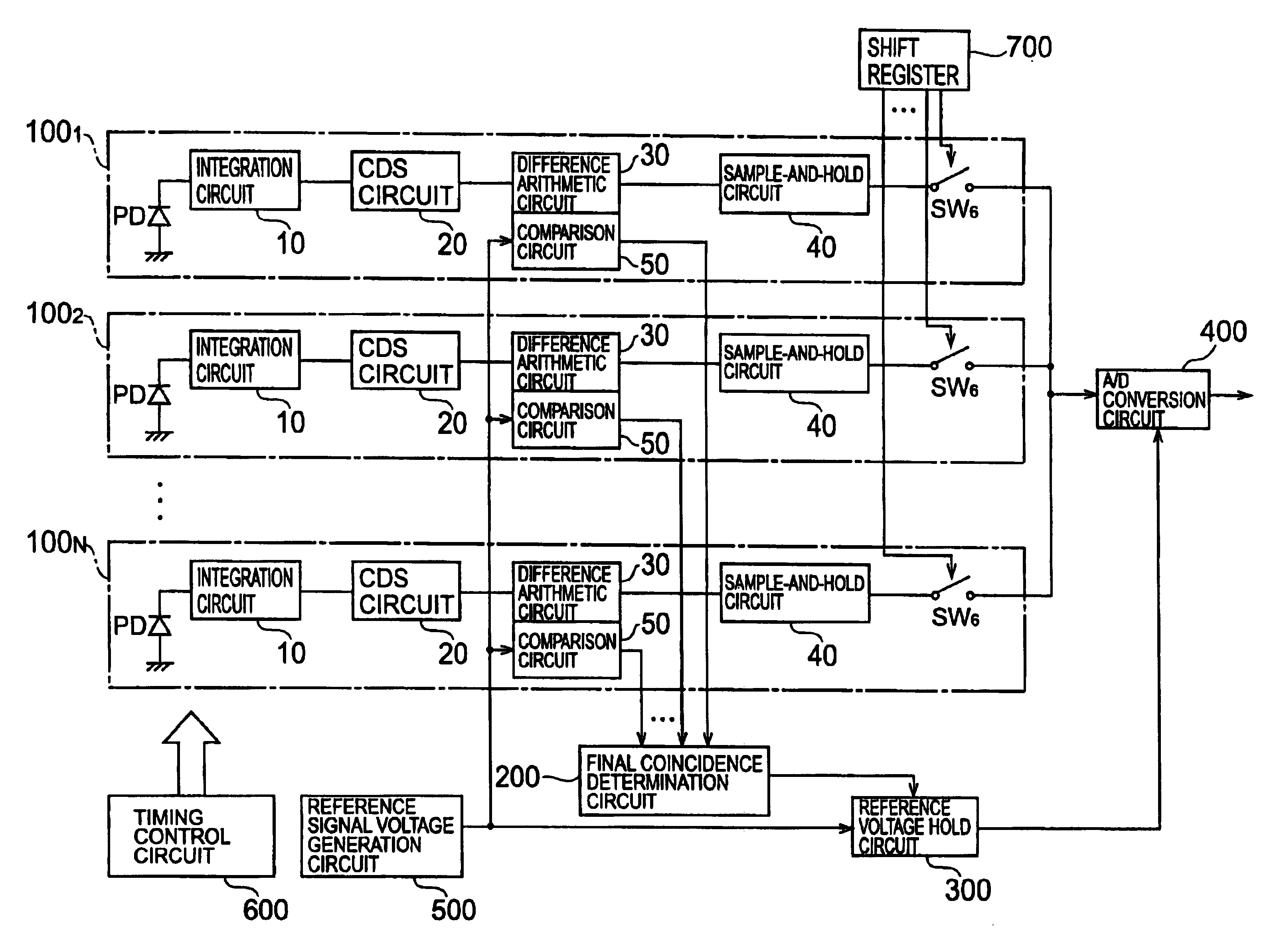
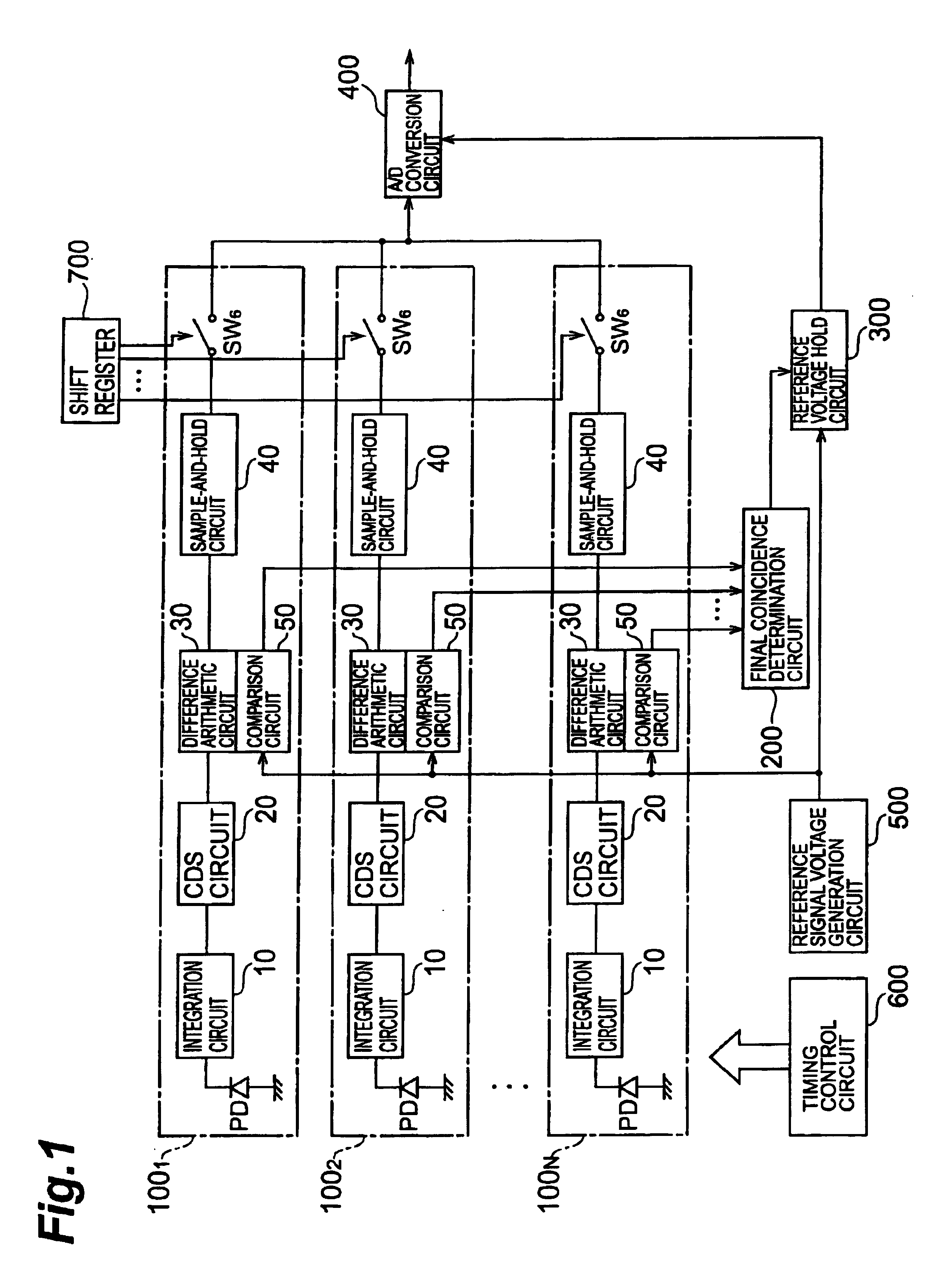
[0034]The arrangement of a solid-state imaging device according to the first embodiment will be described first with reference to FIGS. 1 to 9. FIG. 1 is a schematic view of the overall arrangement of the solid-state imaging device according to the embodiment. The solid-state imaging device according to this embodiment comprises N units 1001 to 100N, a final coincidence determination circuit 200, a reference voltage hold circuit 300, an AID conversion circuit 400, a reference signal voltage generation circuit 500, a timing control circuit 600, and a shift register 700.

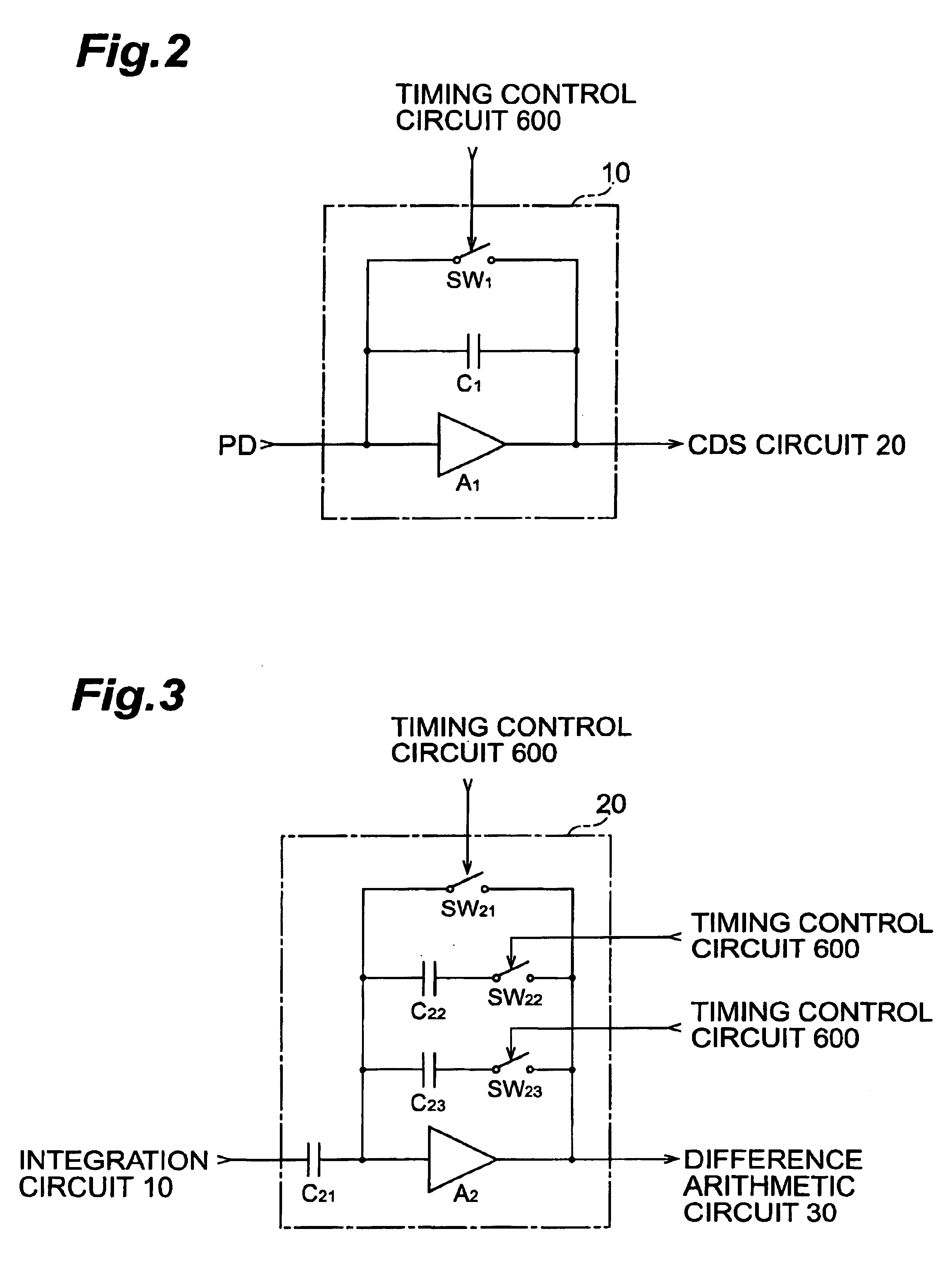
[0035]Each unit 100n includes a photodiode PD, an integration circuit 10, a CDS circuit 20, a difference arithmetic circuit 30, a S-H circuit 40, a comparison circuit 50, and a switch SW6. The integration circuits 10 of the units 100n have identical arrangements. The CDS circuits 20 of the units 100n have identical arrangements. The difference arithmetic circuits 30 of the units 100n have identical ar...

second embodiment

(Second Embodiment)

[0083]The arrangement of a solid-state imaging device according to the second embodiment will be described next. The solid-state imaging device according to the second embodiment is different from the first embodiment in the circuit arrangements of a difference arithmetic circuit 30 and comparison circuit 50. FIG. 12 is a circuit diagram of the difference arithmetic circuit 30 and comparison circuit 50 of the solid-state imaging device according to the second embodiment.

[0084]The difference arithmetic circuit 30 of each unit 100n has a capacitor C3 and amplifier A3 sequentially between the input terminal and the output terminal. The connection point between the capacitor C3 and the amplifier A3 is grounded through a switch SW3. When the switch SW3 is ON, the difference arithmetic circuit 30 stores only charges Q1 in the capacitor C3. When the switch SW3 is OFF, the difference arithmetic circuit 30 removes charges Q2 from the capacitor C3. With this operation, the ...

third embodiment

(Third Embodiment)

[0088]The arrangement of a solid-state imaging device according to the third embodiment will be described next. The solid-state imaging device according to the third embodiment is different from the second is embodiment in the circuit arrangement of a comparison circuit 50. FIG. 13 is a circuit diagram of a difference arithmetic circuit 30 and comparison circuit 50 of the solid-state imaging device according to the third embodiment.

[0089]The comparison circuit 50 of each unit 100n has two input terminals and one output terminal, and also, a switch SW5, capacitor C5, and differential comparator COMP. The non-inverting input terminal of the differential comparator COMP is grounded through the capacitor C5 and also connected, through the switch SW5, to the first input terminal which receives the signal voltage output from the difference arithmetic circuit 30. The inverting input terminal of the differential comparator COMP is connected to the second input terminal whi...


PUM


Abstract

A signal current corresponding to an incident light intensity is output from a photodiode PD, the signal current is converted into a signal voltage by an integration circuit 10, and the amount of a change in signal voltage in a predetermined time is output from a CDS circuit 20. The difference between two voltage values output from the CDS circuit 20 is obtained by a difference arithmetic circuit 30 and held by a S-H circuit 40. In addition, the maximum value of voltage values obtained by the difference arithmetic circuits 30 of respective units 100n is obtained by comparison circuits 50 of the respective units 100n, a reference signal voltage generation circuit 500, a final coincidence determination circuit 200, and a reference voltage hold circuit 300, and on the basis of the maximum value, the A/D conversion range of an A/D conversion circuit 400 is set.

Description

RELATED APPLICATION[0001]This is a continuation-in-part application of application serial no. PCT / JP00 / 05284 filed on Aug. 7, 2000, now pending.BACKGROUND OF THE INVENTION[0002]1. Field of the Invention[0003]The present invention relates to a solid-state imaging device for removing a background light component of light incident on a photodetector and detecting only a signal light component.[0004]2. Related Background Art[0005]A solid-state imaging device has a plurality of photodetectors in a one- or two-dimensional array, in which a signal current output from each photodetector is integrated by an integration circuit, and a signal voltage as an integration result is output. Some solid-state imaging devices convert (A / D-convert) the signal voltage as an analog signal into a digital signal and output the digital signal. If the signal voltage exceeds a predetermined value in this A / D conversion, the digital signal that is A / D-converted and output on the basis of the signal voltage is ...

Claims


Application Information

Patent Timeline
IPC IPC(8): H03M1/18H04N5/217H03M1/12H04N5/335H04N5/355H04N5/357H04N5/363H04N5/378
CPCH03M1/186H04N5/2176H03M1/123H04N25/63
Inventor MIZUNO, SEIICHIROFUNAKOSHI, HARUHIRO
Owner HAMAMATSU PHOTONICS KK
Why Eureka
Try Eureka