Magnetoresistance sensor having an antiferromagnetic pinning layer with both surfaces pinning ferromagnetic bias layers

a magnetoresistance sensor and antiferromagnetic pinning technology, applied in special recording techniques, instruments, nanoinformatics, etc., can solve problems such as exchange coupling and magnetic instability, and achieve the effect of improving the structure efficiency

Inactive Publication Date: 2005-11-01
IBM CORP
View PDF23 Cites 12 Cited by
  • Summary
  • Abstract
  • Description
  • Claims
  • Application Information

AI Technical Summary

Benefits of technology

[0012]The present approach positions the upper antiferromagnetic layer between the upper ferromagnetic layer and the free layer. The upper ferromagnetic layer provides magnetostatic bias to the sensor without a loss of exchange coupling strength between the antiferromagnetic layer and the free layer. With this arrangement of layers, both surfaces of the upper antiferromagnetic layer are employed to pin the adjacent layers, improving the efficiency of the structure. In the GMR sensor, for example, the bottom side of the upper antiferromagnetic layer pins the adjacent portion of the free layer, and the top side of the upper antiferromagnetic layer pins the upper ferromagnetic layer.

Problems solved by technology

The reduction in exchange coupling leads to magnetic instability due to domain formation in the free layer.
The reduced exchange coupling also causes side-reading problems, so that the sensor detects magnetic fields laterally separated from the magnetic track that is in registry with the sensor structure.

Method used


Image

  • Magnetoresistance sensor having an antiferromagnetic pinning layer with both surfaces pinning ferromagnetic bias layers
  • Magnetoresistance sensor having an antiferromagnetic pinning layer with both surfaces pinning ferromagnetic bias layers
  • Magnetoresistance sensor having an antiferromagnetic pinning layer with both surfaces pinning ferromagnetic bias layers

Examples


Embodiment Construction

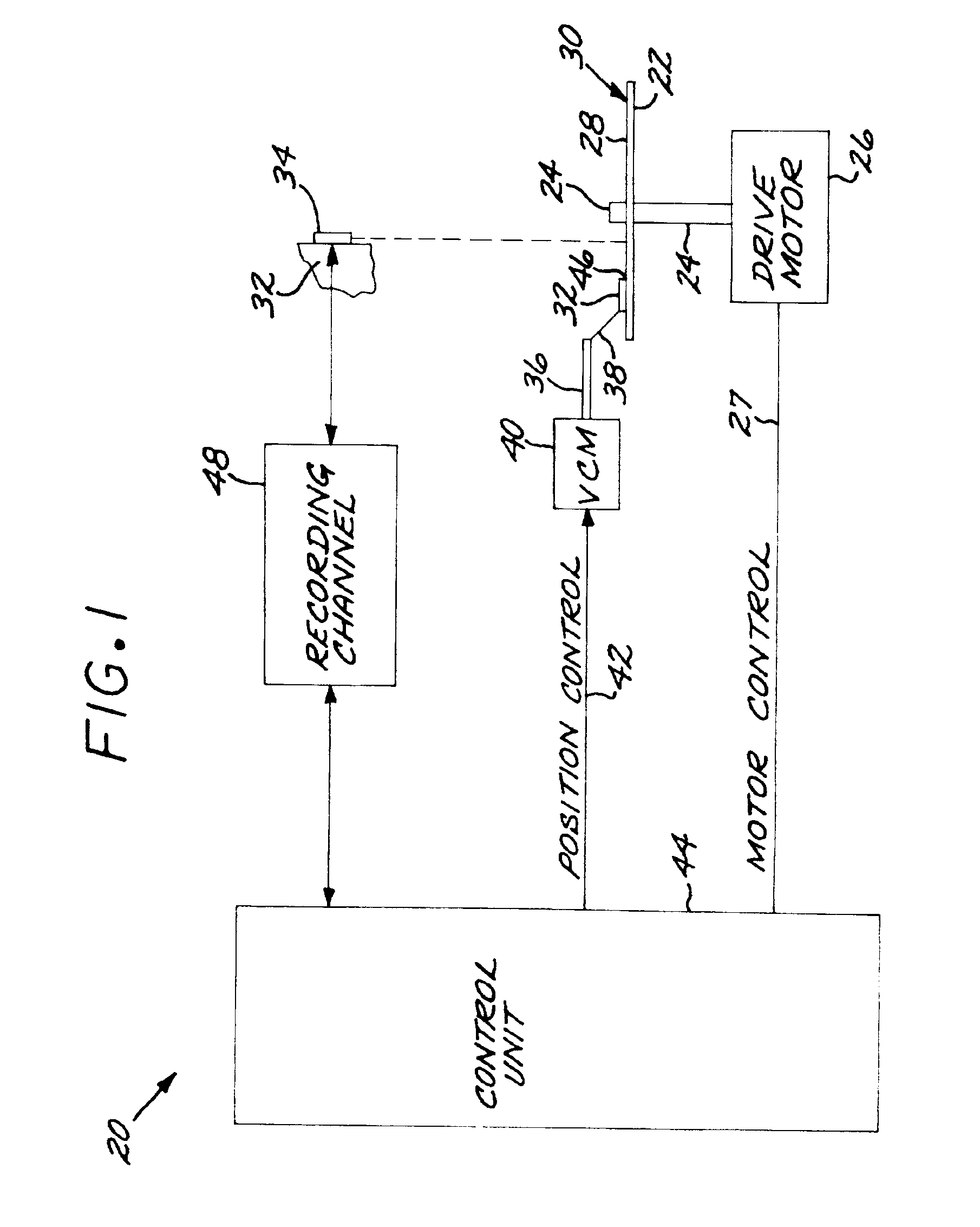
[0019]FIG. 1 shows a data storage system, here depicted as a magnetic disk drive system 20, in which the present approach may be used. The magnetic disk drive system 20 includes a rotatable magnetic storage disk 22 that is supported on a spindle 24 and rotated by a disk drive motor 26 under motor control 27 of a control unit 44. A magnetic storage medium 28 is deposited on a surface 30 of the magnetic storage disk 22.

[0020]A slider 32 is positioned in facing relation to the magnetic storage disk 22. The slider 32 supports at least one read / write head 34 in facing relation to the magnetic storage medium 28 present on the facing surface of the magnetic storage disk 22. The slider 32 is mounted to an actuator arm 36 by a suspension 38. The actuator arm 36 and the slider 32 move radially inwardly and outwardly relative to the magnetic storage disk 22 so that the combined inward / outward motion of the slider 32 and the rotation of the magnetic storage disk 22 allow the read / write head 34 ...


PUM

PropertyMeasurementUnit
thickaaaaaaaaaa
thickaaaaaaaaaa
thickaaaaaaaaaa

Abstract

A magnetoresistance sensor structure includes a magnetoresistance sensor having a sensor surface plane and having a free layer. An upper antiferromagnetic layer overlies at least a portion of the free layer, and an upper ferromagnetic layer overlies and contacts at least a portion of the upper antiferromagnetic layer on a contact face lying parallel to the sensor surface plane, so that the upper antiferromagnetic layer lies between the upper ferromagnetic layer and the free layer. The magnetoresistance sensor may be a giant magnetoresistance sensor or a tunnel magnetoresistance sensor.

Description

[0001]This invention relates to a structure of a magnetoresistance (MR) sensor and, more particularly, to such a sensor having an antiferromagnetic layer above the free layer.BACKGROUND OF THE INVENTION[0002]A magnetoresistance (MR) sensor is used in a read / write head to read magnetic fields on a recording medium of a magnetic storage device. An example is the read / write head of a computer hard disk or a magnetic recording tape drive. The read / write head is positioned closely adjacent to the recording medium, separated from the recording medium by an air bearing surface (ABS) that does not allow them to touch. A data bit is written onto an area of the recording medium using the writing portion of the read / write head by locally changing its magnetic state. That magnetic state is later sensed by the MR sensor to read the data bit.[0003]Two known types of MR sensors are a giant magnetoresistance (GMR) sensor and a tunnel magnetoresistance (TMR) sensor. The general technical basis, cons...

Claims


Application Information

Patent Timeline
Patent Type & Authority Patents(United States)
IPC IPC(8): G01R33/06G01R33/09G11B5/39G11B5/00
CPCB82Y10/00B82Y25/00G01R33/093G11B5/3903G11B5/3909G11B2005/0008G11B2005/0016G11B2005/3996
Inventor GILL, HARDAYAL SINGH
Owner IBM CORP
Why Eureka
Try Eureka