Page buffer having dual register, semiconductor memory device having the same, and program method thereof

a page buffer and register technology, applied in the field of dual register pages, can solve the problem that the time for transmitting data from the cache register b>40/b> to the main register b>30/b> is unnecessarily spent in the normal program operation, and achieve the effect of reducing the whole program time and reducing the program tim

Inactive Publication Date: 2005-11-08
STMICROELECTRONICS SRL +1
View PDF2 Cites 42 Cited by
  • Summary
  • Abstract
  • Description
  • Claims
  • Application Information

AI Technical Summary

Benefits of technology

[0012]The present invention is directed to a page buffer having a dual register which can reduce a whole program time by reducing a program time in a normal program operation, a semiconductor memory device having the same, and a program method thereof.

Problems solved by technology

However, a time for transmitting the data from the cache register 40 to the main register 30 is unnecessarily spent in the normal program operation.

Method used


Image

  • Page buffer having dual register, semiconductor memory device having the same, and program method thereof
  • Page buffer having dual register, semiconductor memory device having the same, and program method thereof
  • Page buffer having dual register, semiconductor memory device having the same, and program method thereof

Examples


Embodiment Construction

[0019]A page buffer having a dual register, a semiconductor memory device having the same, and a program method thereof in accordance with a preferred embodiment of the present invention will now be described in detail with reference to the accompanying drawings. Wherever possible, the same reference numerals will be used throughout the drawings and the description to refer to the same or like parts.

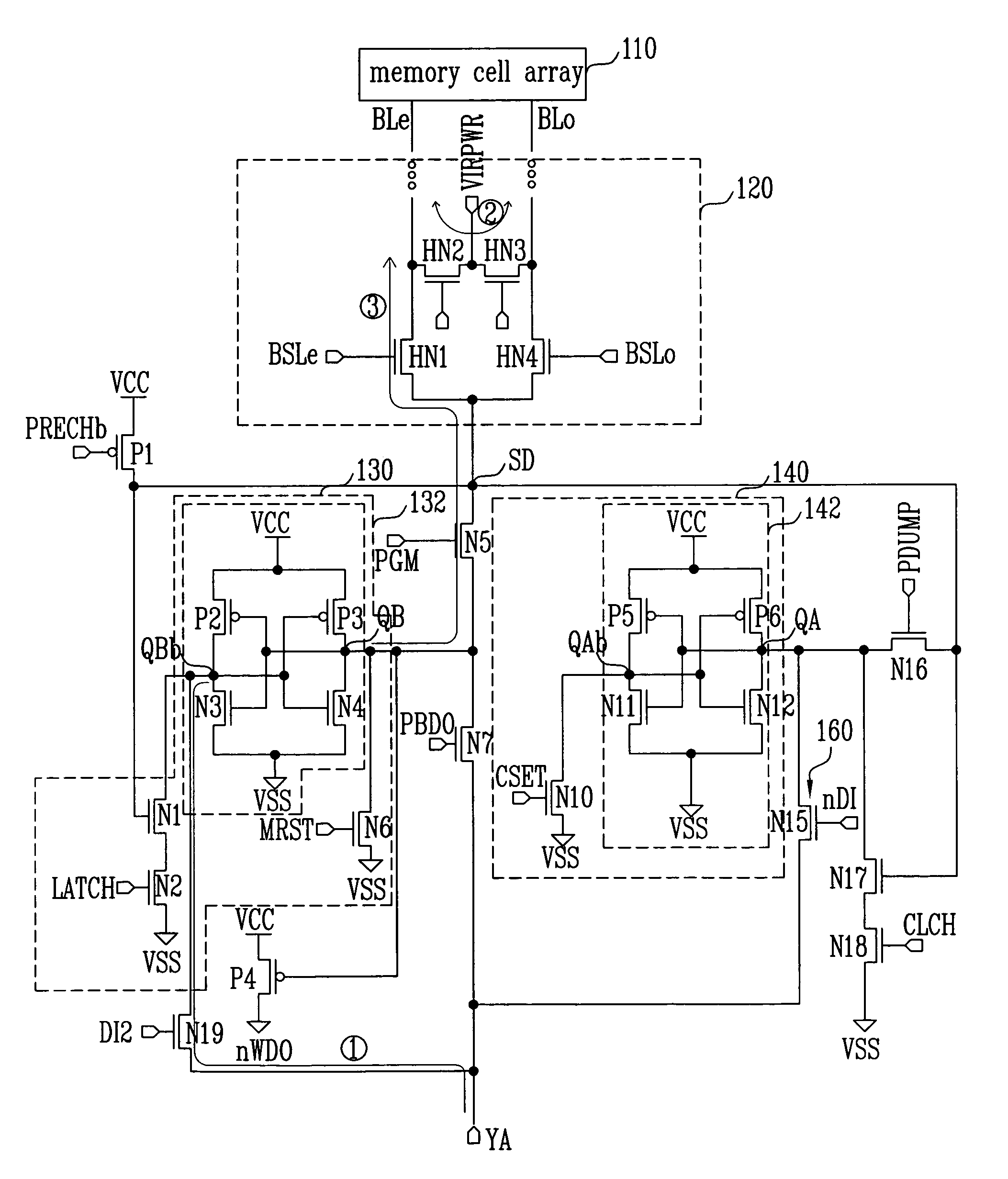
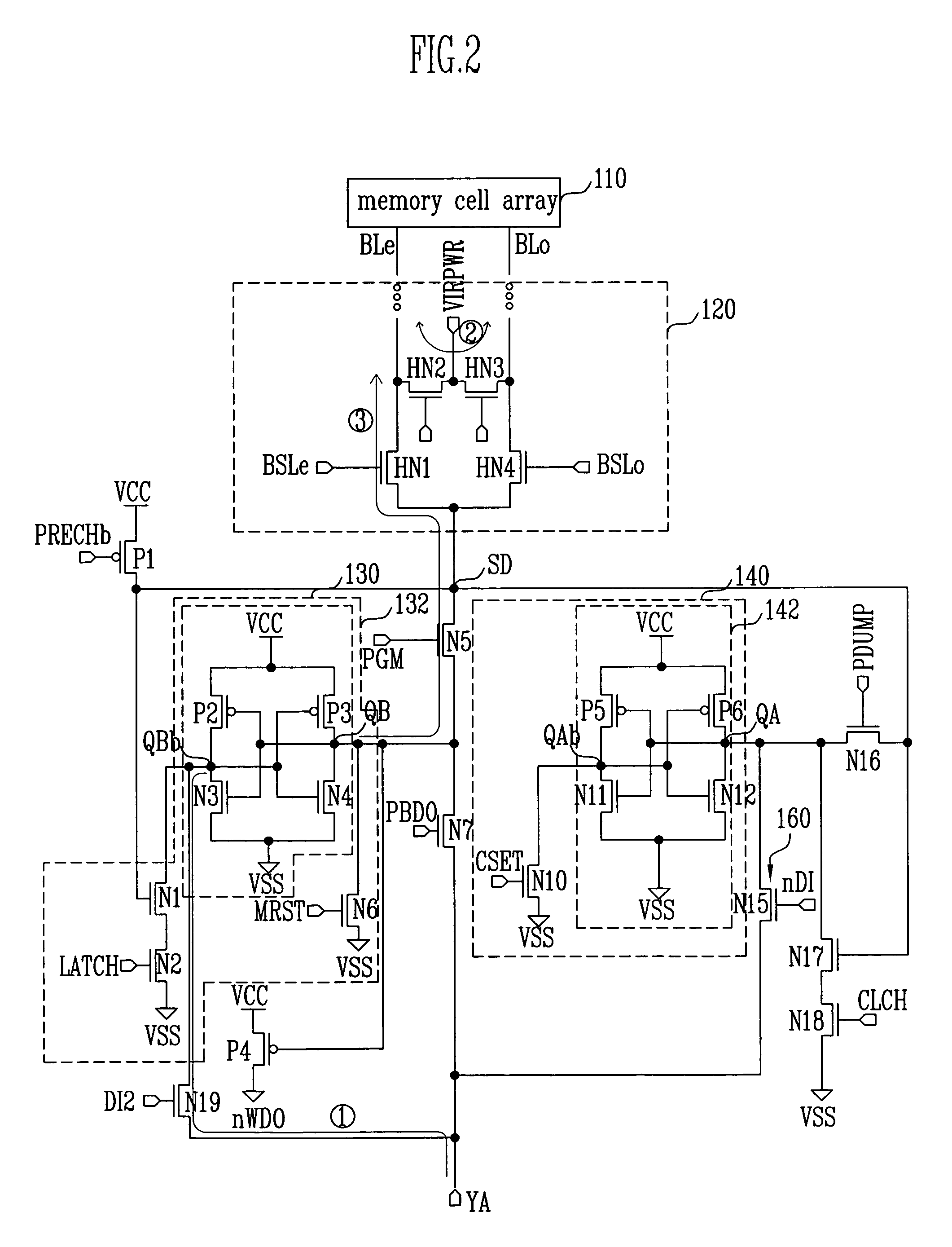
[0020]FIGS. 2 and 3 are circuit diagrams illustrating the page buffer having the dual register in accordance with the preferred embodiment of the present invention.

[0021]As illustrated in FIGS. 2 and 3, the page buffer having the dual register includes a main register 130 and a cache register 140 electrically coupled to a YA pad YA according to operations of switching units 150 and 160. In a program operation, the YA pad YA maintains a ground state. Here, each of the switching units 150 and 160 is operated according to control signals DI2 and nDI individually enabled by an input data in ...


PUM


Abstract

The present invention discloses a page buffer having a dual register, a semiconductor memory device having the same, and a program method thereof. A data transmission path is formed by installing switching units so that a main register as well as a cache register can be directly provided with a data. Therefore, a program operation is performed directly by using the main register in a normal program operation, and by using the cache register in a cache program operation. Accordingly, a process for transmitting the data from the cache register to the main register is omitted in the normal program operation, to reduce a transmission time (about 3 μs). As a result, the program time can be reduced in the whole program operation. Because the process for transmitting the data from the cache register to the main register is omitted in the normal program operation, the circuit control operation can be simplified.

Description

BACKGROUND[0001]1. Field of the Invention[0002]The present invention relates to a page buffer having a dual register, a semiconductor memory device having the same, and a program method thereof, and more particularly to, a page buffer having a dual register which can reduce a whole program time by reducing a program time in a normal program operation, a semiconductor memory device having the same, and a program method thereof.[0003]2. Discussion of Related Art[0004]Recently, there are increasing demands for a semiconductor memory device which has electrical program and erase functions and which does not need a refresh function of re-producing a data at intervals of a predetermined period. In addition, researches have been actively made on a high integration technology of a memory device to develop a large capacity memory device for storing a lot of data. Here, a program operation means an operation of writing a data on a memory cell, and an erase operation means an operation of eras...

Claims


Application Information

Patent Timeline
Patent Type & Authority Patents(United States)
IPC IPC(8): G11C7/00G11C11/34G11C16/02G11C16/04
CPCG11C7/1051G11C7/106G11C7/1078G11C16/10G11C7/1087G11C2216/14G11C16/0483G11C2207/2245A47K10/3631
Inventor JU, GI SEOK
Owner STMICROELECTRONICS SRL
Why Eureka
Try Eureka