Image sensor fabrication method and structure

a technology of image sensor and fabrication method, which is applied in the direction of optics, radio frequency control devices, instruments, etc., can solve the problems of affecting production cycle-time, test-time, yield, and final manufacturing cost, and achieving the effect of reducing the cost of production and maintenance, and improving the quality of the image sensor

Inactive Publication Date: 2005-11-15
TAIWAN SEMICON MFG CO LTD
View PDF8 Cites 26 Cited by
  • Summary
  • Abstract
  • Description
  • Claims
  • Application Information

AI Technical Summary

Benefits of technology

[0011]A method for processing a semiconductor substrate comprises the steps of: providing a substrate having at least one filter region with a plurality of bond pads therein, depositing metal above the bond pads, to re...

Problems solved by technology

If the color filter signal deviation is too large, CMOS image sensor performance may be affected, resulting in yield loss as high as 15 to 20%.
The color filter deposit...

Method used


Image

  • Image sensor fabrication method and structure
  • Image sensor fabrication method and structure
  • Image sensor fabrication method and structure

Examples


Embodiment Construction

[0019]U.S. patent application Ser. No. 10 / 456,759, filed Jun. 6, 2003, is incorporated by reference in its entirety, as though set forth fully herein.

[0020]This description of the exemplary embodiments is intended to be read in connection with the accompanying drawings, which are to be considered part of the entire written description. In the description, relative terms such as “lower,”“upper,”“horizontal,”“vertical,”, “above,”“below,”“up,”“down,”“top” and “bottom” as well as derivative thereof (e.g., “horizontally,”“downwardly,”“upwardly,” etc.) should be construed to refer to the orientation as then described or as shown in the drawing under discussion. These relative terms are for convenience of description and do not require that the apparatus be constructed or operated in a particular orientation. In the drawings, like reference numerals indicate like components or items.

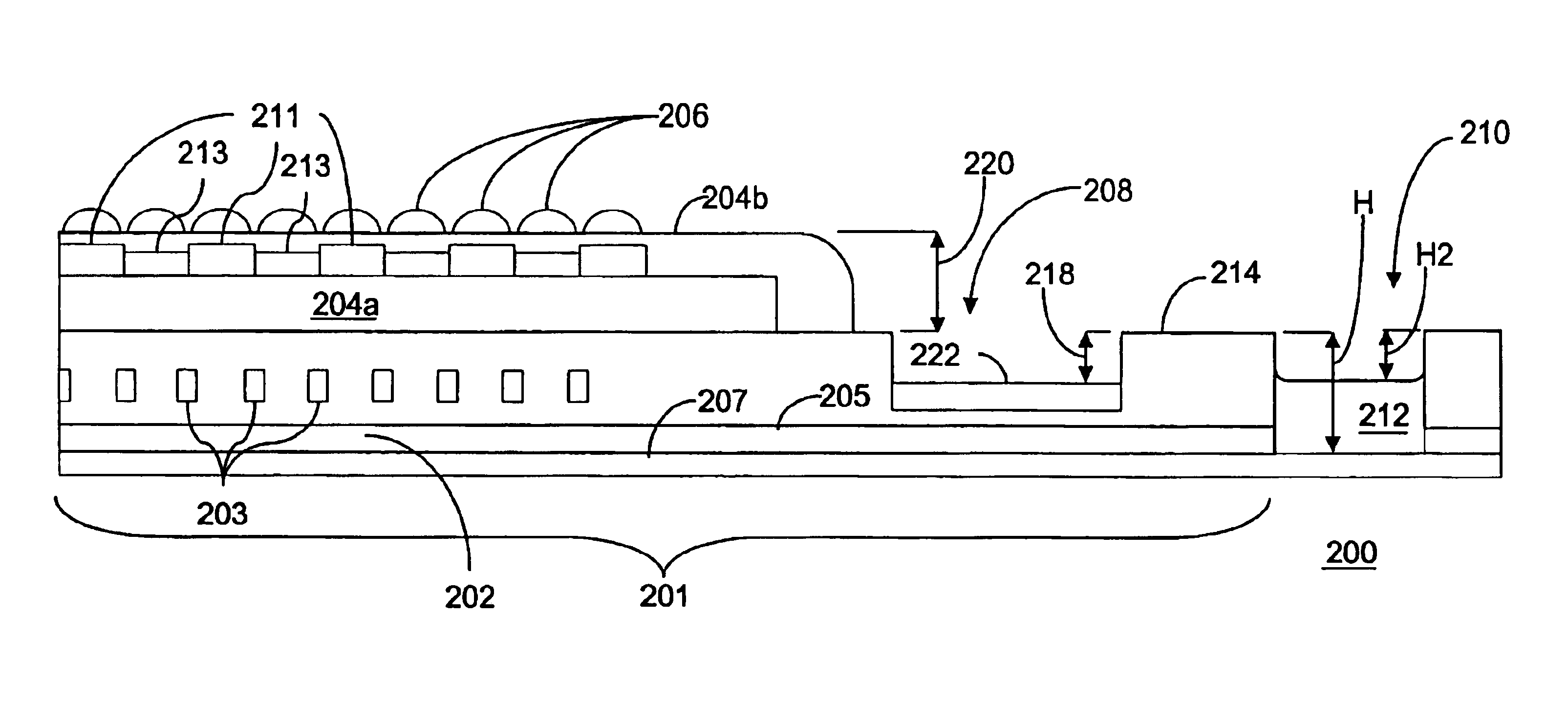
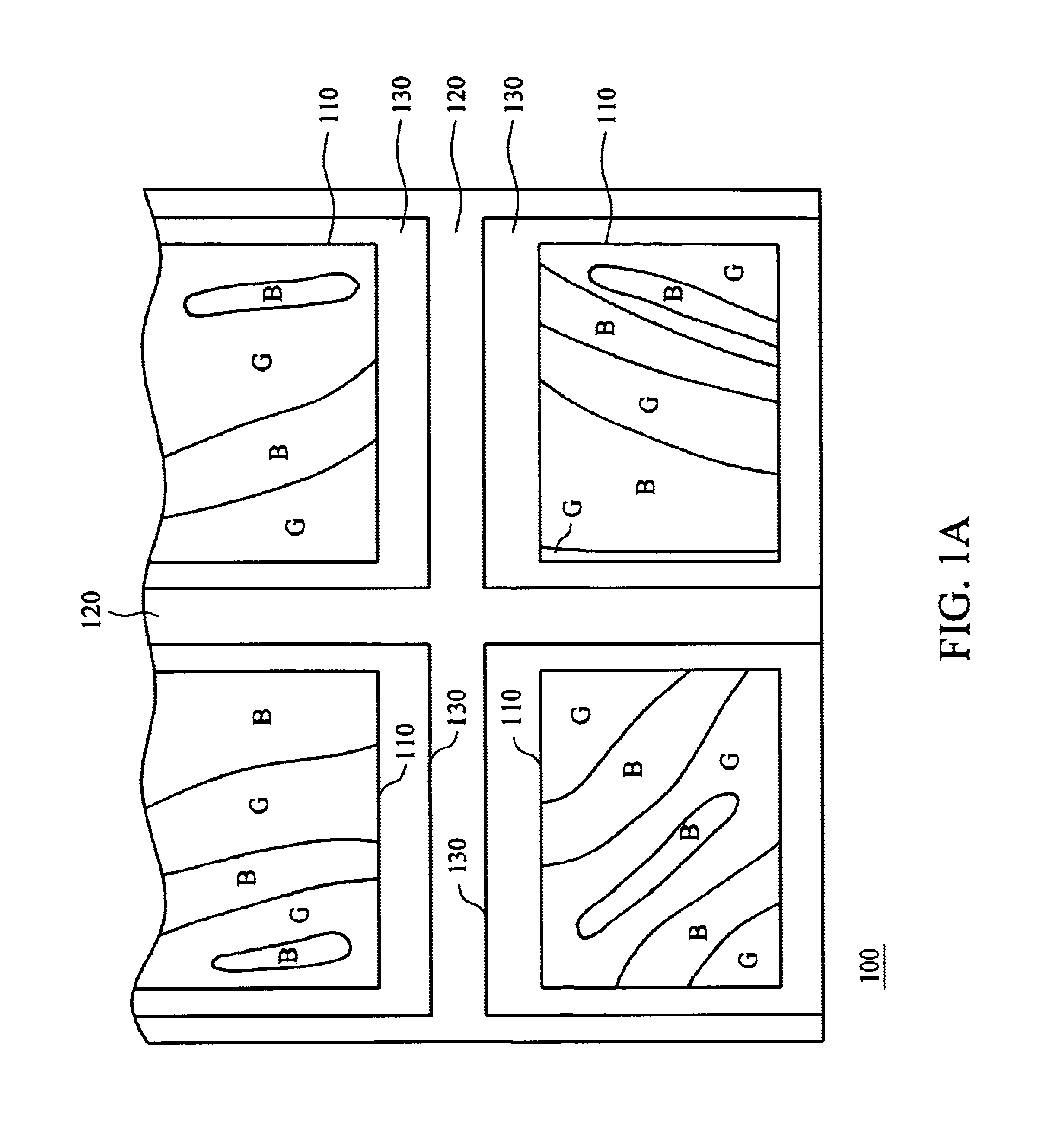
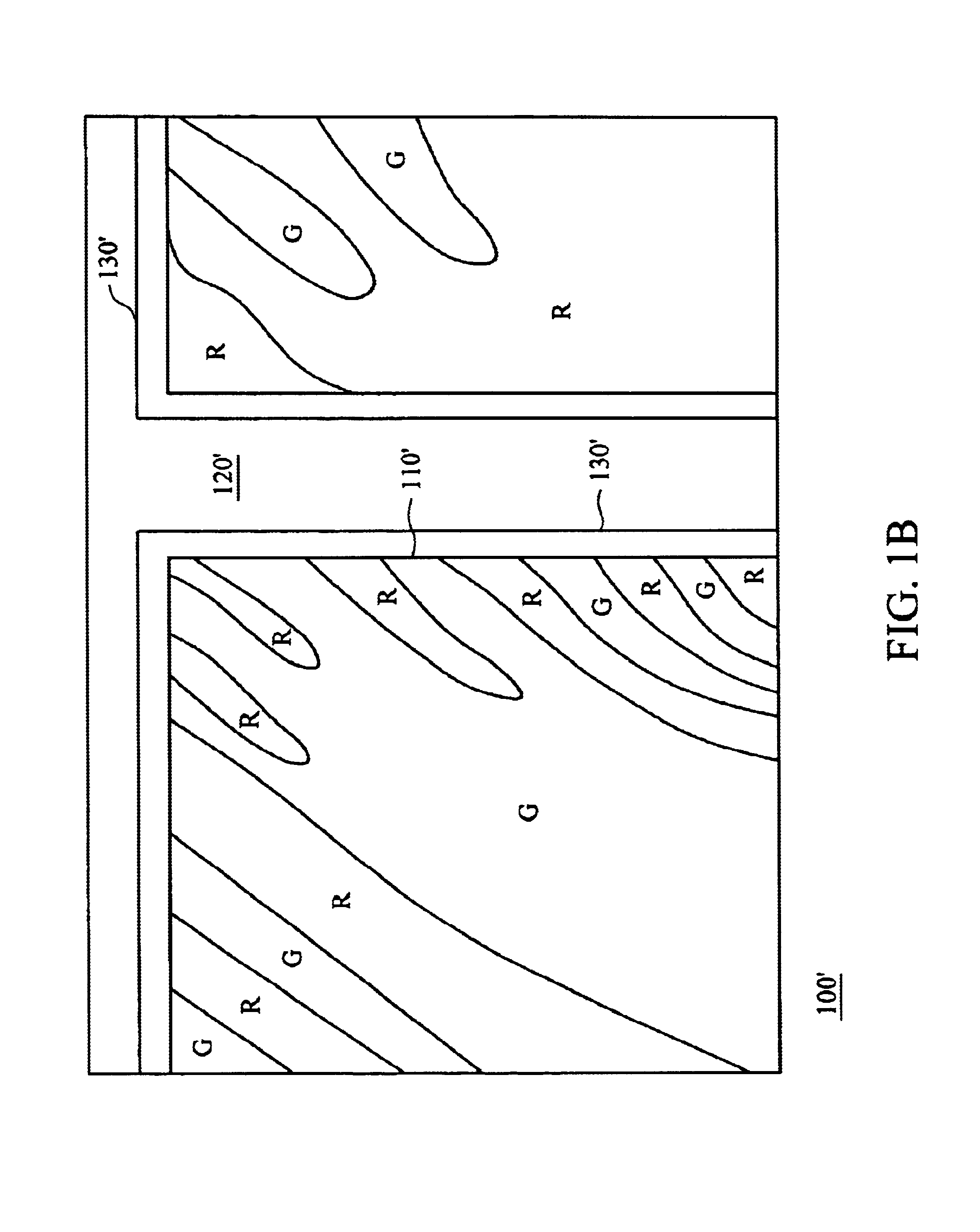
[0021]The inventors have determined that a major factor in causing color signal deviation in color filters i...


PUM


Abstract

A method for processing a semiconductor substrate includes providing a substrate having at least one filter region with a plurality of bond pads in it. Metal is deposited above the bond pads, to reduce the bond pad step height. A planarization layer is formed such that the deposited metal has a height near to a height of the planarization layer. At least one color resist layer is formed above the planarization layer.

Description

[0001]This application is a continuation in part of U.S. patent application Ser. No. 10 / 456,759, filed Jun. 6, 2003.FIELD OF THE INVENTION[0002]The present invention relates to semiconductor devices generally, and more specifically to solid-state color filters.BACKGROUND[0003]Color filters suitable for use in color image sensors have been described in U.S. Pat. Nos. 6,171,885, 6,395,576, 6,274,917, 6,482,669 and 6,495,813, all of which are incorporated by reference herein in their entireties.[0004]A color image sensor is typically a charge-coupled device (CCD) or complementary metal-oxide semiconductor (CMOS) photodiode array structure. The structure includes a spectrally photosensitive layer below one or more layers patterned in an array of color filters, above which resides a surface-layer array of microlens elements. In some conventional configurations, a color pixel is formed using four adjacent pixels on an image sensor. Each of the four pixels is covered by a different color f...

Claims


Application Information

Patent Timeline
IPC IPC(8): H01L29/66H01L21/70H01L21/46H01L21/02H01L29/768H01L21/78H01L27/146
CPCH01L27/14621H01L27/14625H01L27/14685
Inventor KUO, CHIN CHENCHANG, CHIH-KUNGHSU, HUNG-JENWENG, FU-TIENTSENG, TE-FU
Owner TAIWAN SEMICON MFG CO LTD
Why Eureka
Try Eureka