Filter circuit

Inactive Publication Date: 2005-11-15
SATURN LICENSING LLC
View PDF9 Cites 4 Cited by
  • Summary
  • Abstract
  • Description
  • Claims
  • Application Information

AI Technical Summary

Benefits of technology

[0016]The filter circuit constructed as above can be designed smaller by adopting the tri-plate structure in which the distributed parameter design-based resonator conductive patterns are provided inside each of the dielectric insulating layers. In the filter circuit according to the present invention, the plurality of capacitive load patterns is formed along the peripheries of the resonator conductive patterns and the connection between the capacitive load patterns and ground patterns is adjusted, to thereby adjust the filter characteristic by the resonator conductive patterns. Also in the filter circuit according to the present invention, a plurality of capacitive load

Problems solved by technology

In the applications of communications, such as a radio LAN (local area network), in which a frequency in the microwave and millimeter wave bands is used as a carrier frequency, the radio communication module can hardly meet the above-mentioned required specifications such as the small and lightweight design, higher integration and multip

Method used


Image

  • Filter circuit
  • Filter circuit
  • Filter circuit

Examples


Embodiment Construction

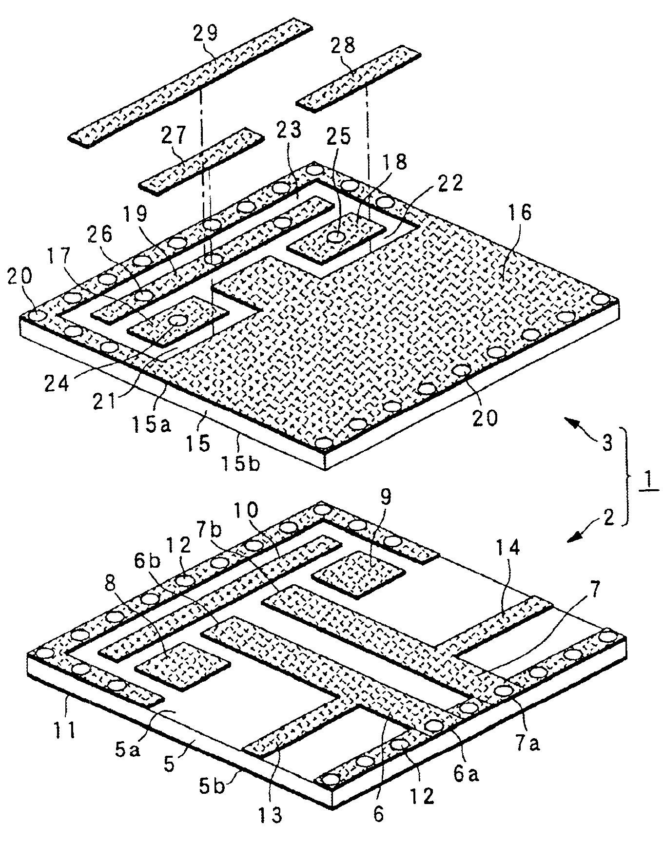
[0029]Referring now to FIGS. 4 and 5, there is illustrated in the forms of an exploded perspective view and an axial-sectional view, respectively, an embodiment of the bandpass filter (BPF) according to the present invention. The BPF is generally indicated with a reference 1. As shown, the BPF 1 includes first and second dielectric substrates 2 and 3 between which there is formed a distributed parameter design-based wiring layer 4. Namely, the BPF 1 is of a so-called tri-plate structure. The BPF 1 is used to form a part of an antenna input / output of a communication module (not shown) to pass a to-be-received or-sent signal superposed on a 5-GHz carrier frequency as in the narrow-band communication system defined in the IEEE 802.11a for example and which is to be sent or received via an antenna.

[0030]The above first dielectric substrate 2 includes a dielectric insulating layer 5 having a predetermined thickness, resonator conductive patterns 6 and 7 formed on a main side 5a of the di...


PUM


Abstract

The present invention provides a small, thin filter circuit showing a desired filter characteristic which is highly accurate, and producible with a high efficiency. The filter circuit includes a pair of dielectric insulating layers 2 and 3, upper and lower, each having a ground pattern 11 (16) formed on the main side thereof, and an inner wiring layer 4 formed between the dielectric insulating layers 2 and 3 and having capacitively coupled resonator conductive patterns 6 and 7 each connected at one end thereof to the ground patterns 11 and 16 via inter-layer connecting vias 12 and open-circuited at the other end. The filter circuit has formed on the inner wiring layer 4 thereof a plurality of capacitive load patterns 8 to 10 laid along the peripheries of the open-circuited end of the resonator conductive patterns 6 and 7 and electrically isolated from the ground pattern 16, and on one of the dielectric insulating layers 2 and 3 thereof correspondingly to each of the capacitive load patterns 8 to 10 a plurality of capacitive load adjusting patterns 17 to 19 electrically isolated from the ground patterns, electrically connected by the inter-layer connecting vias 24 to 26 to each other, and selectively connected to the ground pattern 16.

Description

[0001]This application claim priority to Japanese Patent Application Number JP 2001-283791 filed Sep. 18, 2001 which is incorporated herein by reference.BACKGROUND OF THE INVENTION[0002]1. Field of the Invention[0003]The present invention generally relates to a filter circuit to be provided in a radio communication module for microwave and millimeter wave communications, and more particularly, to a filter circuit adjustable to a predetermined bandpass frequency characteristic.[0004]2. Description of the Related Art[0005]Along with the evolution of the information communication technology, the radio communication module is used in various devices and systems such as mobile communication devices, ISDN (integrated service digital network) or computer devices to enable fast communications of data and information, and a small and lightweight design of them, a higher integration or higher multiplication of their functions. In the applications of communications, such as a radio LAN (local ...

Claims


Application Information

Patent Timeline
IPC IPC(8): H01P1/203H01P1/20H01P1/205
CPCH01P1/20345
Inventor HIRABAYASHI, TAKAYUKI
Owner SATURN LICENSING LLC
Why Eureka
Try Eureka