

Method and apparatus for reducing charge injection in control of MEMS electrostatic actuator array
a technology of electrostatic actuators and control arrangements, applied in the field of microelectromechanical systems) can solve problems such as capacitor pull-in mode capacitor failure to achieve the desired effect,
- Summary
- Abstract
- Description
- Claims
- Application Information
AI Technical Summary
Problems solved by technology
Method used
Image

Examples
first embodiment
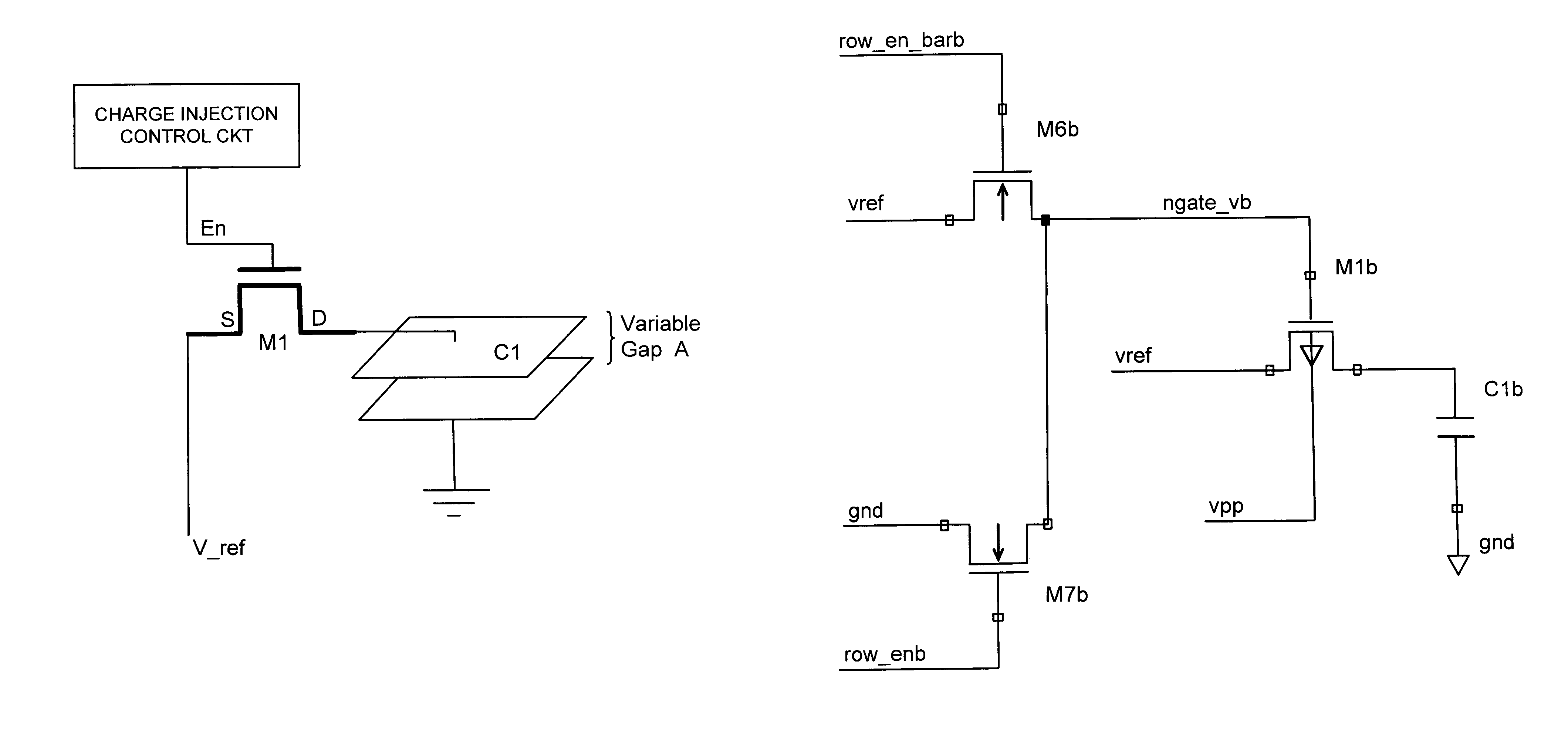
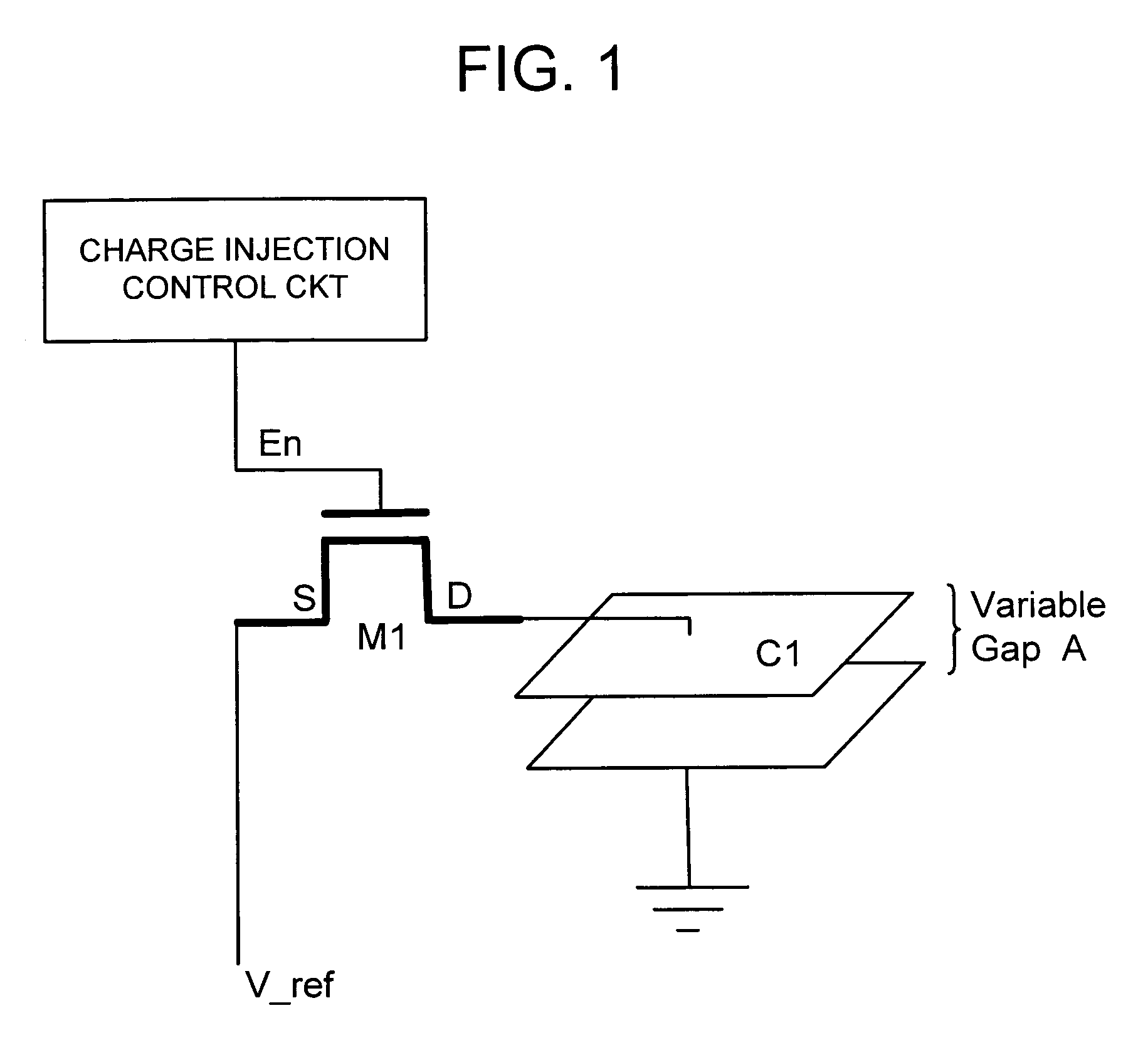
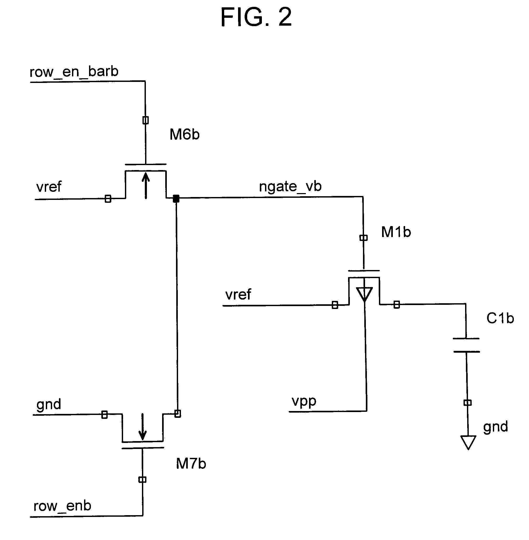
[0028]FIG. 2 shows details of the charge injection control circuit. As will be appreciated, this embodiment requires the addition of two devices to each array subcircuit to limit the “off” gate voltage of the MOS switch and slow the switch closure to the degree that instead of the charge beneath the gate being permitted to distribute 50 / 50 between the source and the drain, most of the charge is, due to the differential capacitance between the source and drain, permitted to drain off to the source side.
[0029]In FIG. 2, M1b and C1b represent M1 and C1 of FIG. 1 respectively. M6b and M7b are used to condition the signal ngate—vb, which enables / disables MOS switch M1b. To turn on M1b (PMOS), M7b (NMOS) is activated by row—enb, a high-voltage signal. When M1b is on, the gate of M1b is driven to all the way to ground (0 V). To turn M1b off, instead of driving the gate of M1b to a full vpp, which would inject maximum coupling noise, the gate of M1b is only driven to vref by M6b. Because th...
second embodiment
[0030]FIG. 3 shows the invention. This embodiment is also directed limiting the “off” gate voltage of the MOS switch and is such that M1c and C1c respectively represent M1 and C1 of FIG. 1. It will be noted that the signal / element designations which end in the letter “b” in FIG. 2 have corresponding designations wherein the letter “b” is replaced with the letter “c”. In FIG. 6, the letter “b” is replaced by the letter “d”. Thus, the high voltage signal row—enb in FIG. 2, becomes row—enc and row—end in FIGS. 3 and 6 respectively.
[0031]The signals row-en and row-en-bar are high voltage signals which are applied in accordance with the need to vary the gap A of the variable capacitors.
[0032]M6c and M7c are used to condition the signal ngate—vc, which enables / disables NMOS switch M1c. When M1c (NMOS) is turned on, M7c (PMOS) is activated by row—en—barc, a high-voltage signal. To turn M1c on, the gate of M1c is driven to a full high voltage vpp. To turn M1c off, instead of driving the gat...
third embodiment
[0037]FIG. 6 shows the charge injection control circuit. This embodiment is directed limiting both “on” and “off” gate voltages to the MOS switch and includes the addition of two devices and one or two reference voltages to each array subcircuit. The reference voltages can be common to the entire array and the embodiment utilizes a PMOS analog switch.
[0038]In FIG. 6, the reference voltages v—gate—off and v—gate—on can be set depending on the range of voltages that will be used for vref. For example, v—gate—on could be set to approximately one volt below the minimum vref, and v—gate—off could be set to approximately the maximum vref, thus ensuring that the accumulation charge (when M1d is off) and inversion charge (when M1d is on) are minimized.
[0039]The operation of the circuit shown in FIG. 6 was verified using the same set of conditions as were used in FIGS. 4 and 5. FIG. 7 shows simulation results from the circuit of FIG. 6. The bottom waveform is row—end, the middle waveform is ...
PUM
 Abstract
Description
Claims
Application Information