

Charge pump circuit
a pump circuit and discharge pump technology, applied in the direction of power conversion systems, dc-dc conversion, instruments, etc., can solve the problems of reducing transistor reliability and voltage conversion efficiency, and achieve the effect of high reliability and increased voltage conversion efficiency
- Summary
- Abstract
- Description
- Claims
- Application Information
AI Technical Summary
Benefits of technology
Problems solved by technology
Method used
Image

Examples
first embodiment
[First Embodiment]
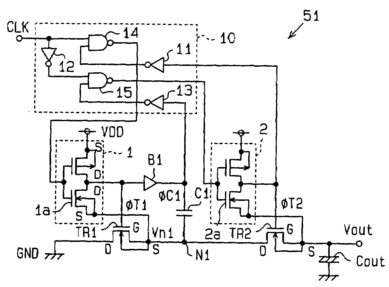
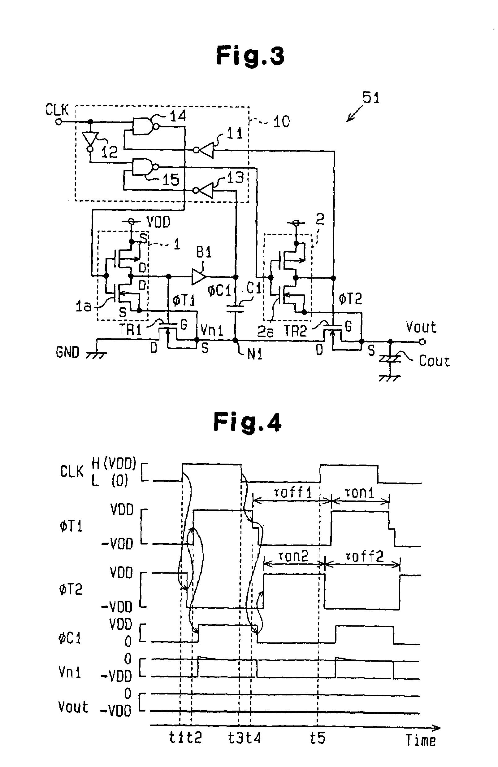
[0029]FIG. 3 is a schematic circuit diagram of a charge pump circuit 51 according to a first embodiment of the present invention. The charge pump circuit 51 converts a power supply voltage VDD to −VDD (logic value), which is a negative voltage, and includes two switching transistors TR1, TR2, which are preferably n-channel MOS transistors, a capacitor C1, and an output capacitor Cout, The sources S and drains D of the switching transistors TR1, TR2 are inverted in accordance with the operational status of the transistors TR1, TR2.
[0030]The charge pump circuit 51 further includes a timing adjustment circuit 10, CMOS inverters 1, 2, and a buffer circuit B1, which serves as a delay circuit.
[0031]The timing adjustment circuit 10 includes inverters 11, 12, 13 and NAND circuits 14, 15. The timing adjustment circuit 10 receives a clock signal CLK. Based on the clock signal CLK, the timing adjustment circuit 10 generates control clock signals ØT1, ØT2, which respectively a...
second embodiment
[Second Embodiment]
[0048]A charge pump circuit 52 according to a second embodiment of the present invention will now be described centering on parts differing from the charge pump circuit 51 of the first embodiment.
[0049]FIG. 5 is a schematic circuit diagram of the charge pump circuit 52 of the second embodiment. The charge pump circuit 52 has a timing adjustment circuit 20 that differs from the timing adjustment circuit 10 of the charge pump circuit 51 of the first embodiment. The charge pump circuit 52 includes four switching transistors TR1, TR2, TR3, TR4 and three capacitors C1, C2, C3 and converts the power supply voltage VDD to negative voltage −3VDD (logic value). The sources S and drains D of the switching transistors TR1, TR2, TR3, TR4 are inverted in accordance with the operational conditions of the transistors TR1, TR2, TR3, TR4.
[0050]The timing adjustment circuit 20 includes three inverters 21, 22, 23 and two NOR circuits 24, 25. The timing adjustment circuit 20 adjusts ...
third embodiment
[Third Embodiment]
[0065]A charge pump circuit 53 according to a third embodiment of the present invention will now be described centering on parts differing from the charge pump circuit 51 of the first embodiment.
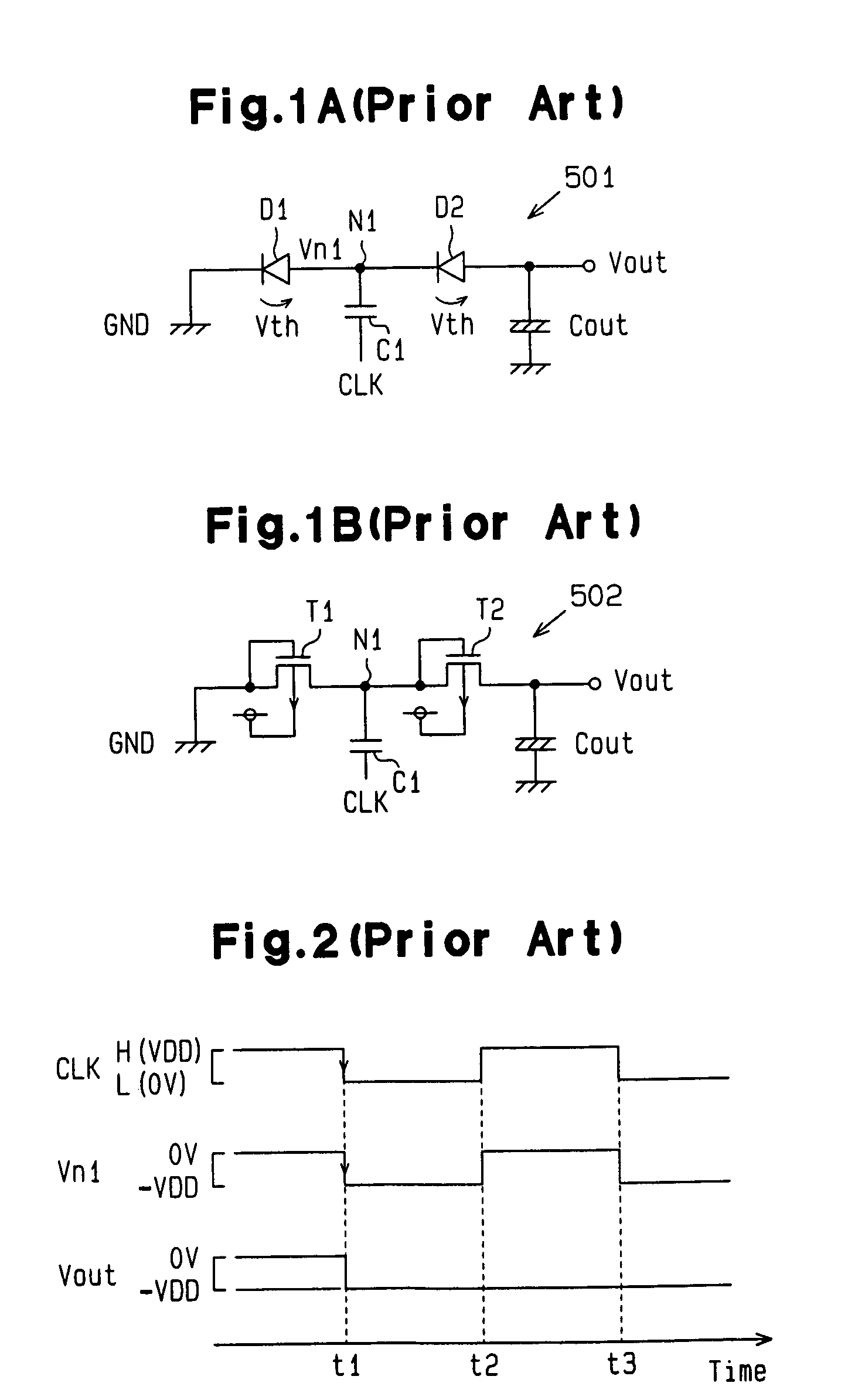
[0066]The charge pump circuit 51 of the first embodiment is provided with the buffer circuit B1, which delays the control clock signal ØT1 by a predetermined time to generate the capacitor clock ØC1. The buffer circuit 51 changes the source voltage (voltage at node N1) Vn1 after the gate voltage of the switching transistor TR1 is determined. This avoids the influence of parasitic transistor on the transistor TR1.
[0067]In this case, unnecessary current consumption may occur from when the transistor TR1 goes on to when the signal output by the buffer circuit B1 goes high. In other words, the transistor TR1 goes on thereby connecting the drain and source of the transistor TR1 This causes current to flow from the GND to node N1 and increases the potential Vn1 at the node N1. As...
PUM
 Abstract
Description
Claims
Application Information