Display and method of manufacturing the same

a technology of display and manufacturing method, applied in the field of display, can solve the problems of low necessity of deterioration of display contrast, and unnecessary increase in cost, so as to reduce the need for performing such a high-precision color filter fabricating process, increase contrast, and simplify the manufacturing process

Inactive Publication Date: 2005-12-06
SONY CORP
View PDF20 Cites 19 Cited by
  • Summary
  • Abstract
  • Description
  • Claims
  • Application Information

AI Technical Summary

Benefits of technology

[0014]The invention has been achieved in consideration of the above problems and its object is to provide a display of a type that emits light from a second electrode side, capable of increasing contrast by suppressing external light reflection by a wiring electrode between organic EL devices and realizing a simplified manufacturing process and reduction in cost, and a method of manufacturing the same.
[0017]In the display and the method of manufacturing the display according to the invention, the red, green, and blue filters are formed by printing and at least two filters out of the red, green, and blue filters are overlapped with each other by printing, thereby forming the black matrix so as to face the boundary region of the organic EL devices. Therefore, by the simple manufacturing process, the color filters and the black matrix having performance necessary and sufficient for the organic EL display can be formed at low cost.

Problems solved by technology

A display using such organic EL devices has a problem such that external light reflection by the organic EL devices and a wiring electrode between the devices is large and the contrast of the display deteriorates.
Forming a black matrix equivalent to that in a liquid crystal display in an organic EL display causes unnecessary increase in cost.
However, in an organic EL display, the necessity of performing such a high-precision color filter fabricating process is low.
Further, the material itself of a color filter is expensive and its cost makes up a considerable part of a liquid crystal display.
However, it has been pointed out that the configuration has a narrow alignment margin and it is difficult to apply the invention at least to a liquid crystal display (Japanese Patent Laid-Open Nos. 2000-29014 and 2000-89215).
Since two layers of resin of the same color are stacked in the pixel portion, patterning by lithography has to be performed total six times in order to form two pattern layers of color filters of three colors, and the like, the manufacturing processes are too complicated from the viewpoints of performance and characteristics required for the color filters of an organic EL display, and an effect at reducing the cost which is the most important subject right now is poor.

Method used


Image

  • Display and method of manufacturing the same
  • Display and method of manufacturing the same
  • Display and method of manufacturing the same

Examples


first embodiment

[First Embodiment]

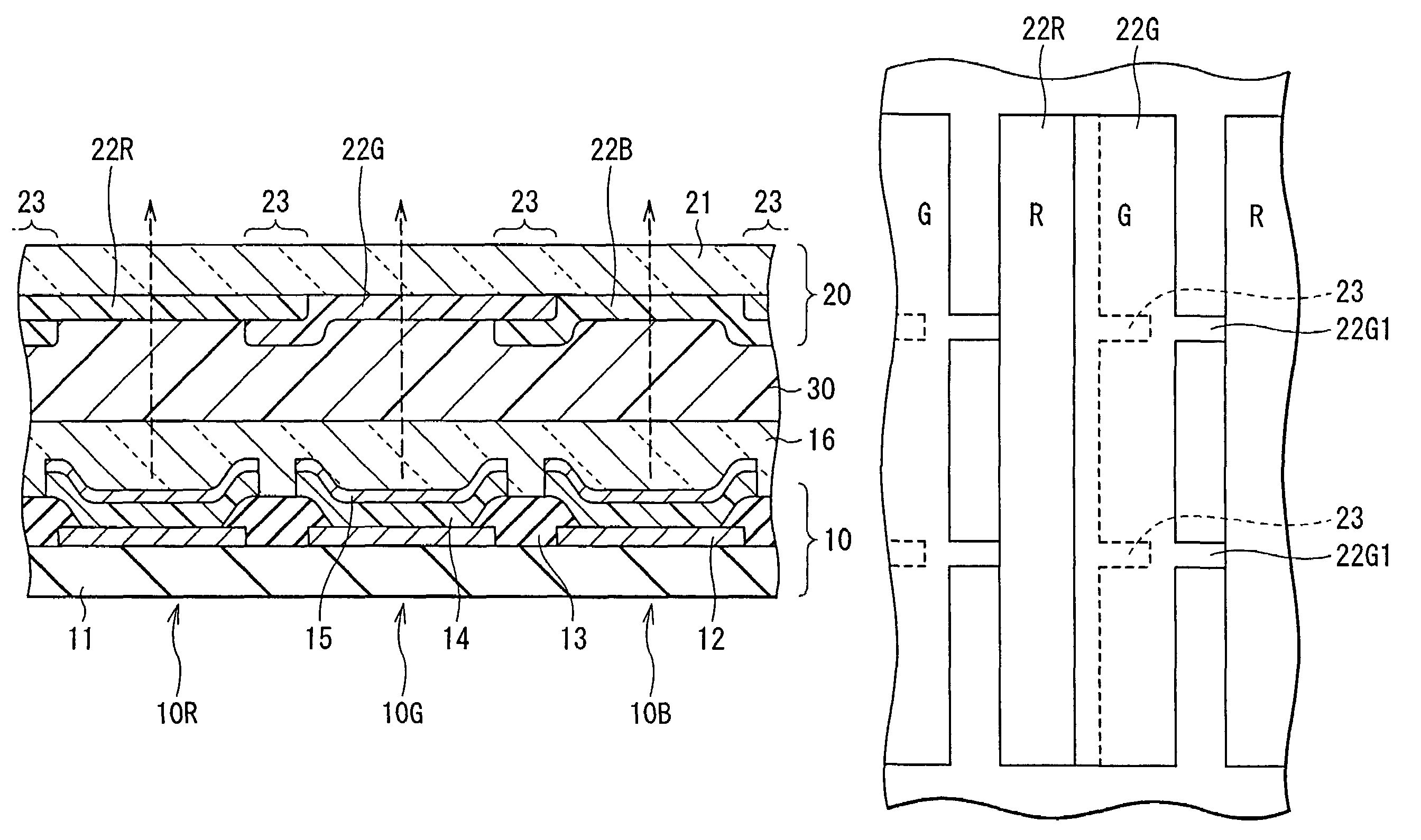
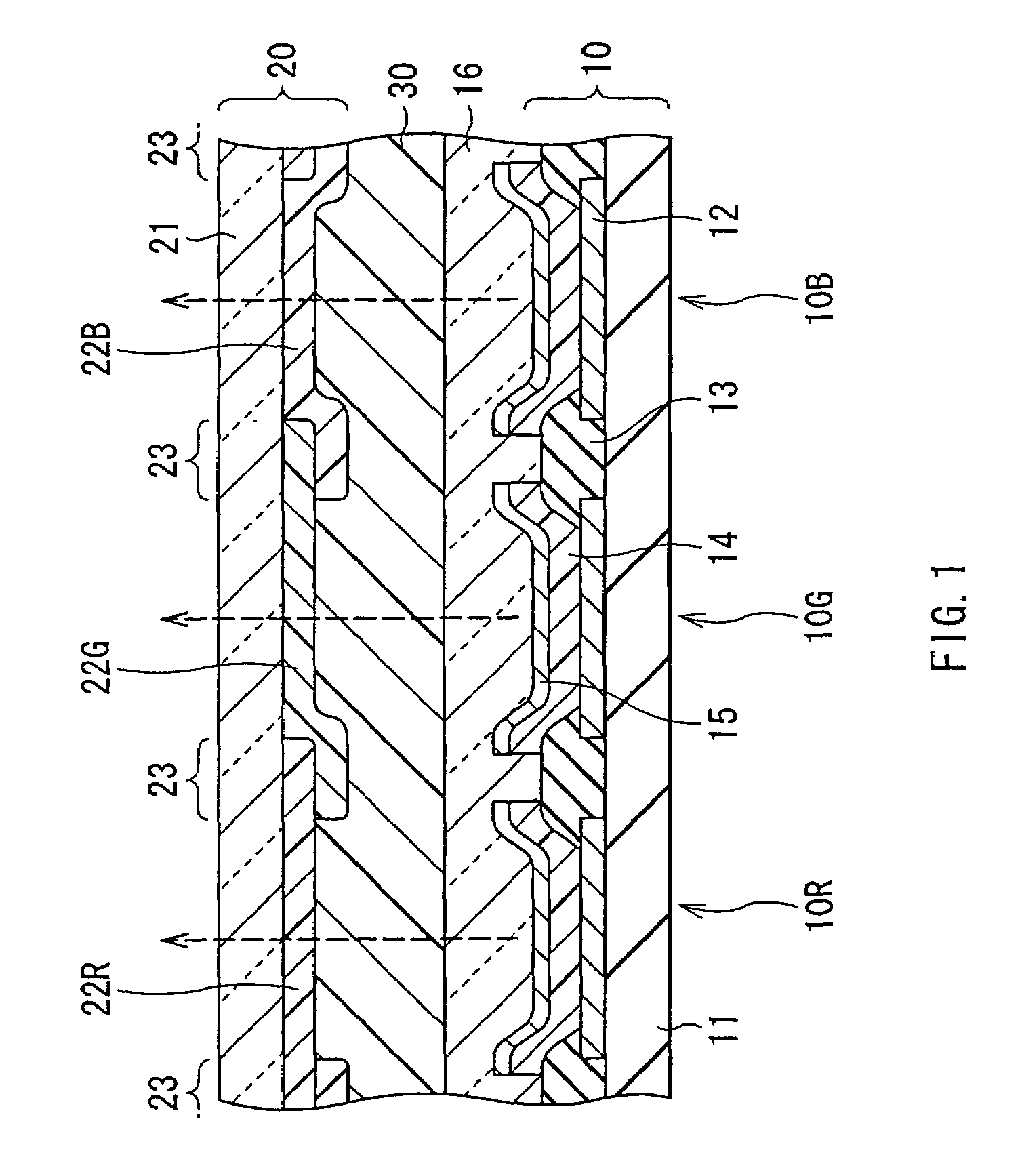
[0032]FIG. 1 shows a sectional structure of a display according to a first embodiment of the invention. The display is used as an organic EL color display of a very thin type. In the display, for example, a driving panel 10 and a sealing panel 20 are disposed so as to face each other and their whole surfaces are adhered to each other with an adhesive layer 30 in between. In the driving panel 10, for example, on a substrate 11 for driving made of an insulating material such as glass, an organic EL device 10R emitting red light, an organic EL device 10G emitting green light, and an organic EL device 10B emitting blue light are provided in order in a matrix as a whole.

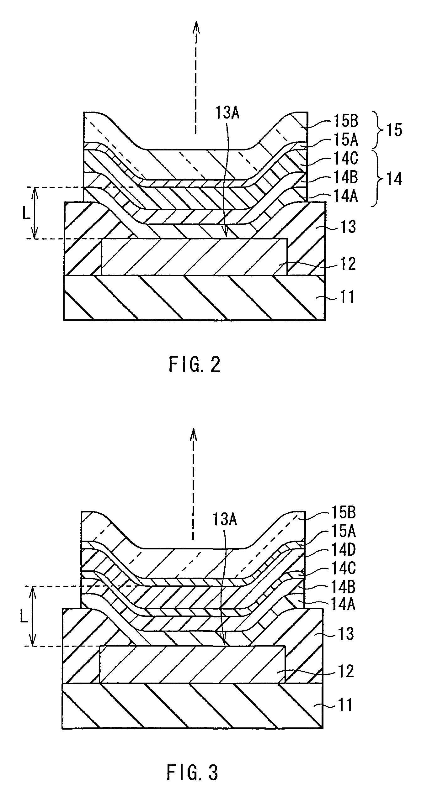
[0033]Each of the organic EL devices 10R, 10G, and 10B has a structure in which, for example, an anode 12 as a first electrode, an insulating layer 13, an organic layer 14, and a cathode 15 as a second electrode are stacked in this order on the substrate 11 for driving. The organic EL devices 10R, 10G, a...

second embodiment

[Second Embodiment]

[0062]A display according to a second embodiment of the invention will now be described. The display is the same as that described with reference to FIGS. 1 to 3 in the first embodiment except that the red, green, and blue filters 22R, 22G and 22B are disposed in stripes as shown in FIG. 9. Therefore, the same reference numeral is designated to the same component and its detailed description will not be repeated.

[0063]In the display, the red, green, and blue filters 22R, 22G and 22B are formed in stripes by printing. The black matrix 23 is provided between the neighboring stripes of the different colors and is also provided at predetermined intervals in the stripes of each color. With the configuration, as shown by an alternate long and short dash line in FIG. 9, a pixel 25 is formed by the neighboring red, green, and blue filters 22R, 22G and 22B.

[0064]Concretely, as shown in the cross section of FIG. 10B, for example, the filter 22B of blue as a complementary co...

third embodiment

[Third Embodiment]

[0070]FIG. 12 shows a display according to a third embodiment of the invention. The display is the same as that described in the first embodiment except that an antireflection film 24 is provided on the surface opposite to the driving panel 10 of the substrate 21 for sealing. The same component is designated by the same reference numeral and its detailed description will not be repeated.

[0071]The antireflection film 24 is used to prevent surface reflection of external light in the substrate 21 for sealing. In the case where the substrate 21 for sealing is made of, for example, glass, its surface reflectivity is about 4%. When external light reflection in the display is suppressed by the red, green, and blue filters 22R, 22G, and 22B, the black matrix 23, and the like, the surface reflection in the substrate 21 for sealing cannot be ignored.

[0072]The antireflection film 24 is preferably constructed by, for example, a thin film filter in which silicon oxide (SiO2), t...


PUM


Abstract

The invention provides a display of a type of getting light out of a second electrode side, capable of increasing contrast by suppressing external light reflection, simplifying a manufacturing process, and reducing cost, and a method of manufacturing the same. A substrate for driving is provided with organic electroluminescence (EL) devices for getting light out of a cathode side. A red filter, a green filter, and a blue filter are formed on a substrate for sealing by printing so as to face the organic EL devices. By overlapping at least two filters out of the red, green, and blue filters by printing, a black matrix is formed so as to face the boundary region of the organic EL devices, so that external light reflection by a wiring electrode between the devices is suppressed.

Description

[0001]The present application is a divisional of U.S. application Ser. No. 10 / 299,652, filed Nov. 19, 2002, which claims priority to Japanese Patent Application No. JP2001-372949, filed Dec. 6, 2001, and Japanese Patent Application No. JP2002-305463, filed Oct. 21, 2002. The subject matter of U.S. application Ser. No. 10 / 299,652 is incorporated herein by reference.BACKGROUND OF THE INVENTION[0002]1. Field of the Invention[0003]The present invention relates to a display having a plurality of organic electroluminescence (EL) devices in which a first electrode, at least one organic layer including a luminescent layer, and a second electrode are sequentially stacked, and getting light generated in the luminescent layer out of the second electrode side, and a method of manufacturing the same.[0004]2. Description of the Related Art[0005]Conventionally, a display using a self-emitting device such as a light emitting diode (LED), a laser diode (LD), or an organic electroluminescence device ...

Claims


Application Information

Patent Timeline
Patent Type & Authority Patents(United States)
IPC IPC(8): G02B5/20H01L27/32H01L51/50H01L51/52H05B33/02H05B33/04H05B33/10H05B33/12H05B33/22H05B33/24
CPCH01L27/322H01L51/5284H01L51/524H01L51/5262H01L51/5265H01L2251/5315H10K59/38H10K50/852H10K50/841H10K50/85H10K50/865H10K2102/3026H05B33/22
Inventor URABE, TETSUOYAMADA, JIROSASAOKA, TATSUYA
Owner SONY CORP
Why Eureka
Try Eureka