Electrifying method and manufacturing method of electron-source substrate

a manufacturing method and technology of electron-source substrate, applied in the manufacture of electric discharge tubes/lamps, electromechanical systems, cold cathode manufacturing, etc., can solve the problems of limiting the effect of stress relaxation and the temperature difference between top and bottom surfaces of substrates, and achieve the effect of preventing a substrate from cracking

Inactive Publication Date: 2005-12-06
CANON KK
View PDF10 Cites 28 Cited by
  • Summary
  • Abstract
  • Description
  • Claims
  • Application Information

AI Technical Summary

Benefits of technology

[0021]It is an object of the present invention to provide an electrifying method capable of preventing a substrate from cracking due to a temperature difference between an electrifying region (heating region) of the substrate and the circumferential region thereof.
[0022]It is another object of the present invention to provide a manufacturing method and a manufacturing device of an electron-source substrate that achieve improvements in characteristics and in yield of an electron-emission element.
[0023]It is still another object of the present invention to provide a manufacturing method of a planar shape image-forming apparatus excellent in image quality.
[0038]According to an electrifying method of the present invention, the substrate can be effectively prevented from cracking due to the temperature difference of the substrate between an electrifying region (heating region) and a circumferential region. For example, by applying it to a manufacturing process of an electron-source substrate and an image-forming apparatus, improvement in image quality (activation with high duty), improvement in a value added to a product (small-width frame structure), and cost down (yield and productivity) are achieved.

Problems solved by technology

There may be a technique for relaxing the stress by cooling the bottom surface of the electron-emission element forming region on the electron-source substrate while heating the periphery; however, since the heat is recovered in the thickness direction of the substrate, with increasing duty, the temperature difference between top and bottom surfaces of the substrate increases, so that there is a limit to the effect of stress relaxation.

Method used


Image

  • Electrifying method and manufacturing method of electron-source substrate
  • Electrifying method and manufacturing method of electron-source substrate
  • Electrifying method and manufacturing method of electron-source substrate

Examples


examples

[0108]The present invention will be described below in detail by exemplifying specific examples; however, the present invention is not limited to the examples and various modifications in design and element exchanges can be made within the scope in that the object of the present invention can be achieved.

first example

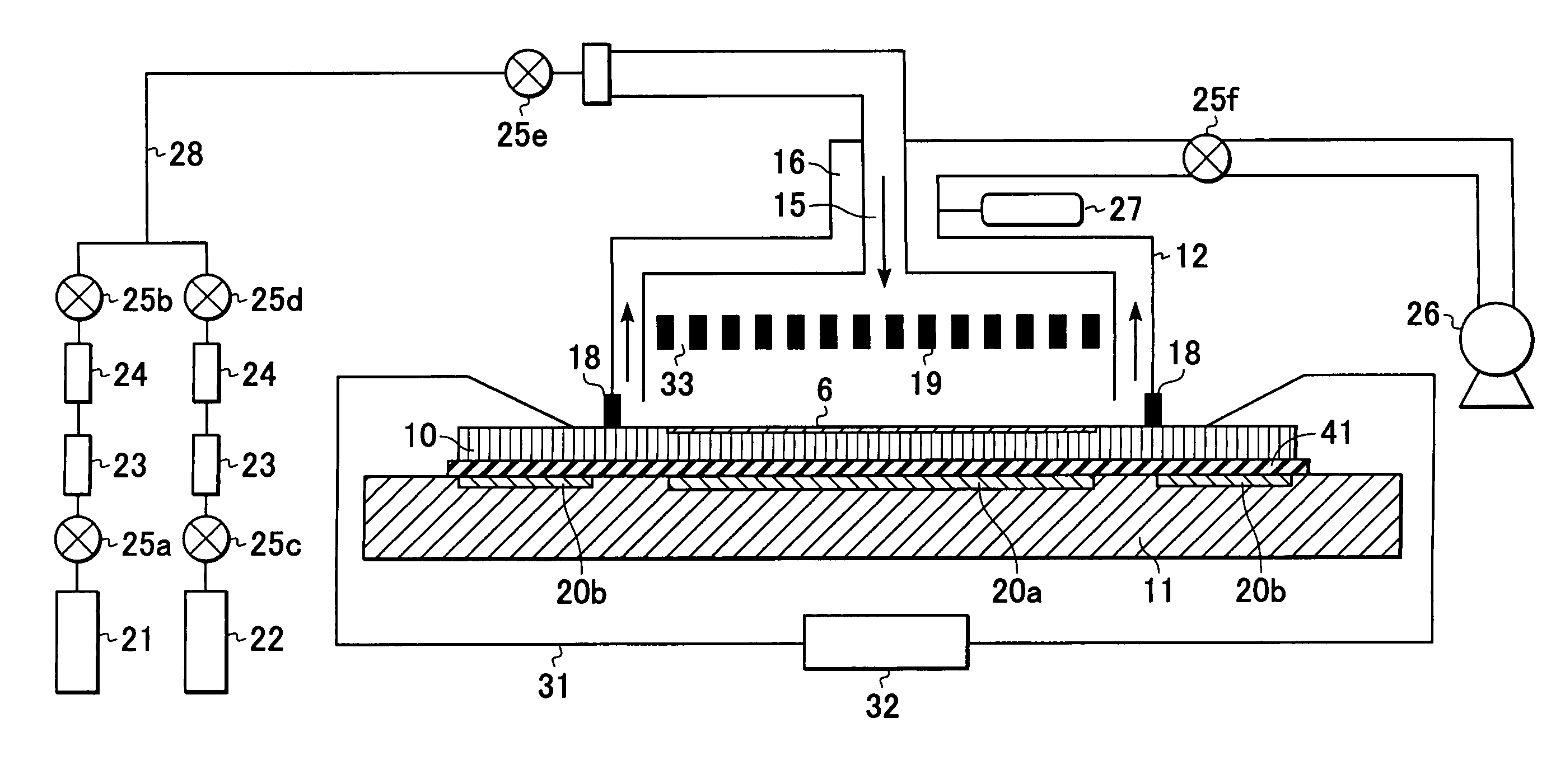
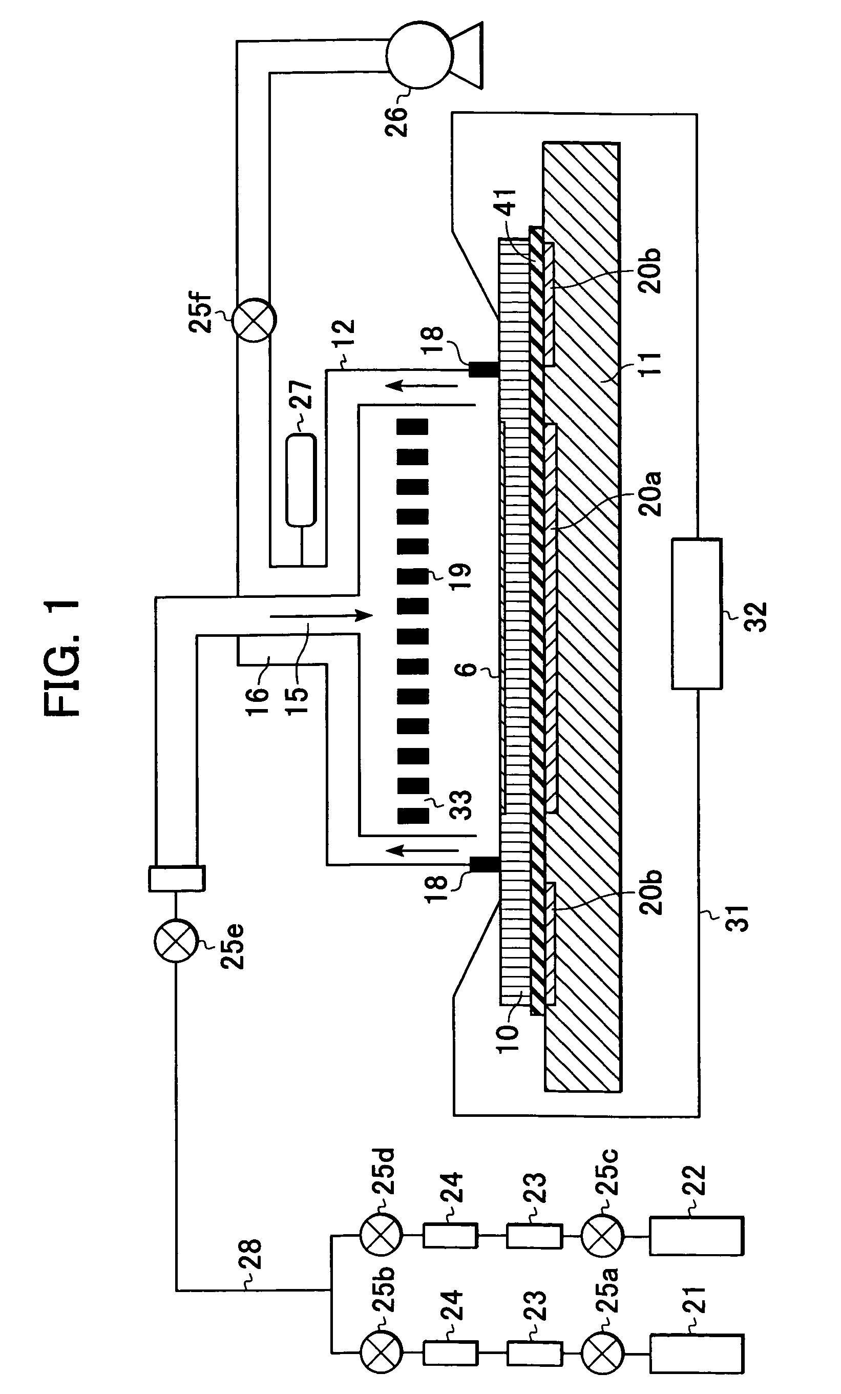
[0109]A first example is a method for manufacturing an electron-source substrate, shown in FIG. 8, having a plurality of surface-conduction electron-emission elements shown in FIGS. 6 and 7 with a manufacturing device according to the present invention. Referring to FIGS. 6 to 8, numeral 10 denotes a substrate; numerals 2 and 3: element electrodes; numeral 4: a conductive film; numeral 29: a carbon film; numeral 5: a clearance between the carbon films 29; and symbol G denotes a gap between the conductive films 4.

[0110]On the glass substrate 10 (350 mm×300 mm in size, 2.8 mm in thickness) made by depositing SiO2 layers, Pt (platinum) paste was printed by offset printing so as to form element electrodes 2 and 3, shown in FIG. 9, with a thickness of 50 nm by baking it. Also, by screen printing, Ag (silver) paste was printed and baked so as to form X-direction wiring 7 (240 pieces) and Y-direction wiring 8 (720 pieces). On the crossing section of the X-direction wiring 7 with the Y-dire...


PUM


Abstract

A method according to the present invention is for electrifying a plurality of electric conductors arranged on a substrate including the step of setting an average temperature difference during electrifying processing between a region S0 in that the plurality of electric conductors on the substrate are arranged and a circumferential region S1 of the region S0 at 15° C. or more, and the substrate satisfies the relational expression:L1 / L0>EαΔT / σth−1.where L0[m]: the width of the region S0 L1[m]: the width of the region S1 ΔT[K]: the average temperature differenceE[Pa]: the Young's modulus of the substrateα[ / K]: the coefficient of linear thermal expansion of the substrateσth[Pa]: the material constant of the substrate.

Description

BACKGROUND OF THE INVENTION[0001]1. Field of the Invention[0002]The present invention relates to a method for electrifying a plurality of electric conductors arranged on a substrate, and in particular relates an electrifying method capable of preventing cracks of the substrate produced by a temperature difference of the substrate during the electrifying. Furthermore, it relates to a manufacturing method and a manufacturing device of an electron-source substrate having a plurality of electron-emission elements as well as a manufacturing method of an image-forming apparatus on the basis of the electrifying method.[0003]2. Description of the Related Art[0004]Hitherto, as the electron-emission element, two kinds of elements using a thermal electron-emission element and a cold cathode electron-emission element are known as a general classification. The cold cathode electron-emission element generally includes a field emission type, a metal / insulting layer / metal type, and a surface-conduc...

Claims


Application Information

Patent Timeline
Patent Type & Authority Patents(United States)
IPC IPC(8): H01J9/02
CPCH01J9/027H01J9/24H01J2329/00
Inventor AZUMA, HISANOBU
Owner CANON KK
Why Eureka
Try Eureka