Multi-finger transistor

a multi-finger transistor and transistor structure technology, applied in semiconductor devices, semiconductor/solid-state device details, electrical devices, etc., can solve the problems of affecting the miniaturization of the device, affecting the protection function affecting the lateral area of the multi-finger transistor, so as to prevent the damage of the drain region

Active Publication Date: 2005-12-06
UNITED MICROELECTRONICS CORP
View PDF2 Cites 7 Cited by
  • Summary
  • Abstract
  • Description
  • Claims
  • Application Information

AI Technical Summary

Benefits of technology

[0009]Accordingly, this invention provides a multi-finger transistor that includes a special drift region structure for simultaneously switching on all parasitic BJTs on an ESD event to prevent damage of the drain regions of the central transistors.
[0011]In the multi-finger transistor of this invention, a drain region accompanying with a drift region wider in the side direction has a higher breakdown voltage, so that the breakdown current from the drain region to the substrate is smaller. Therefore, the substrate currents from the drains of the transistors more distant from the pick-up region are smaller, thereby compensating the effect of the higher base resistance of the parasitic BJTs. Consequently, each parasitic BJT can be switched on at the same time to evenly share the ESD current, so that the ESD protection function of the multi-finger transistor can be assured. Moreover, since no additional substrate / well pick-up region is disposed in the multi-finger transistor of this invention, the lateral area of the multi-finger transistor is not increased in this invention.

Problems solved by technology

In accompany with continuous reduction in dimensions, IC devices, especially the gate oxide layers therein, ate more and more easily damaged by ESD.
Consequently, most of the ESD current will flow through the central NMOS, and contact spiking or junction punch easily occurs to the drain region thereof to significantly deteriorate the ESD protection function of the multi-finger transistor.
However, by distributing the well / substrate contacts in the source region, the lateral area of the multi-finger transistor is significantly increased to adversely affect the device miniaturization.

Method used


Image

  • Multi-finger transistor
  • Multi-finger transistor
  • Multi-finger transistor

Examples


Embodiment Construction

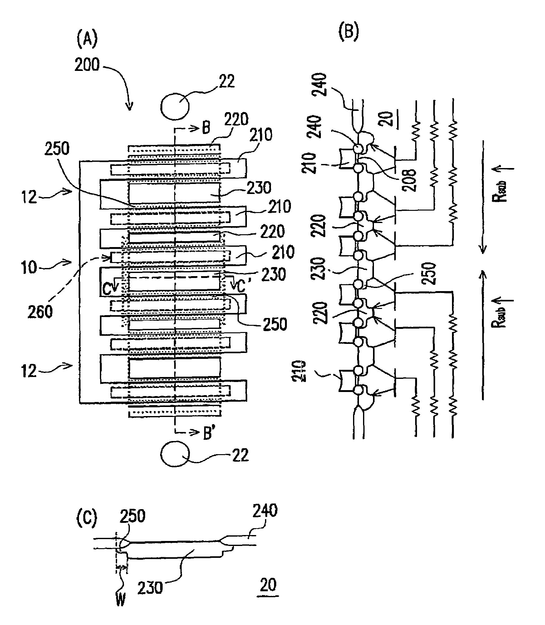
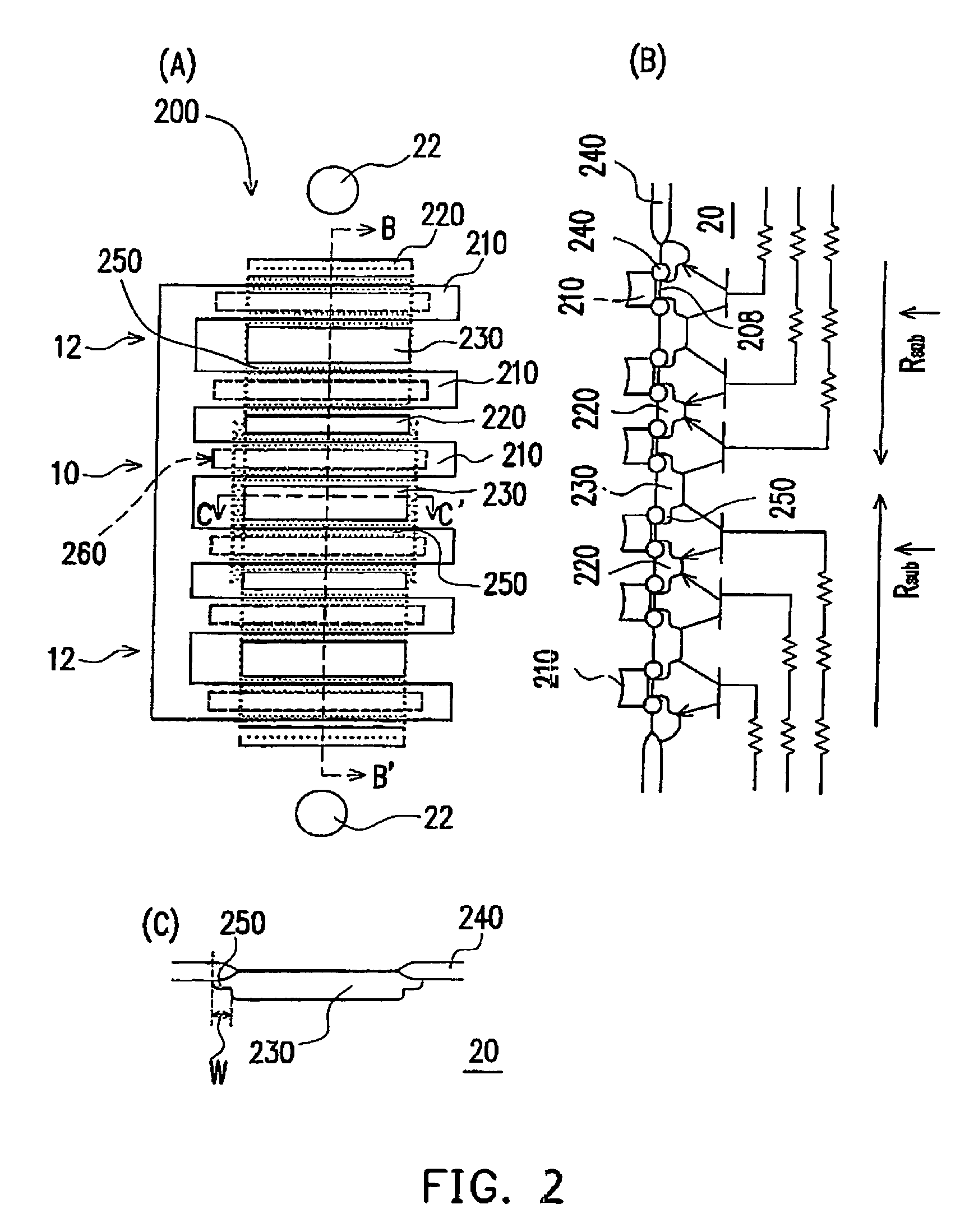
[0018]FIGS. 2(A), (B) and (C) illustrate a multi-finger transistor according to the preferred embodiment of this invention in a top view, in B–B′ cross-sectional view and in C–C′ cross-sectional view, respectively.

[0019]Referring to FIG. 2, the multi-finger transistor 200 is disposed on a P-well (or P-substrate) 20, including multiple parallel gates 210, N-doped source regions 220, N-doped drain regions 230, a field oxide layer 240 and drift regions 250. The P-well 20 further includes two pick-up regions 22 at two sides of the multi-finger transistor 200 along the arrangement direction of the parallel transistors. The gates 210 are connected to each other at the ends of the same side, and are separated from the P-well 20 by gate dielectric layers 208 overlying channel regions 260. The source regions 220 and the drain regions 230 are located in the P-well 20 between the parallel gates 210, and are arranged alternately in the P-well 20. A drain region 230 or a non-terminal source regi...


PUM


Abstract

A multi-finger transistor is described, including multiple parallel transistors. Each transistor includes a gate dielectric layer, a gate, a source / drain region, and a drift region in the peripheral substrate of the source / drain region separating the source / drain region and the channel region under the gate. The width of the drift region extending from the side boundary of the source / drain region increases stepwise from the edge sections of the multi-finger transistor toward the central section of the same.

Description

BACKGROUND OF THE INVENTION[0001]1. Field of the Invention[0002]The present invention relates to a structure of a semiconductor device. More particularly, the present invention relates to a structure of a multi-finger transistor that is suitably used as an electrostatic discharge (ESD) protection device.[0003]2. Description of the Related Art[0004]In accompany with continuous reduction in dimensions, IC devices, especially the gate oxide layers therein, ate more and more easily damaged by ESD. Therefore, additional ESD protection devices are usually designed in integrated circuits. One type of ESD protection device is the multi-finger transistor, which is usually constituted of multiple NMOS transistors.[0005]FIGS. 1(A), (B) and (C) illustrate a conventional multi-finger transistor in a top view, in B–B′ cross-sectional view and in C—C′ cross-sectional view, respectively. As shown in FIG. 1, the conventional multi-finger transistor 100 is formed on a P-substrate 10, including gates ...

Claims


Application Information

Patent Timeline
Patent Type & Authority Patents(United States)
IPC IPC(8): H01L21/266H01L23/62H01L29/06H01L29/08H01L29/78H01L29/94
CPCH01L29/0692H01L29/0847H01L29/7833H01L21/266H01L2924/0002H01L2924/00
Inventor CHENG, JYH-NAN
Owner UNITED MICROELECTRONICS CORP
Why Eureka
Try Eureka