Self-timed scan circuit for ASIC fault testing

a self-timed scan and fault technology, applied in the direction of pulse technique, instruments, computation using denominational number representation, etc., can solve the problems of double-sided surface mount techniques, fine-pitch technology packages, and difficulty in device testing, and achieve the effect of reducing the difficulty of testing high-density electronic systems with traditional test methods

Inactive Publication Date: 2005-12-06
AVAGO TECH WIRELESS IP SINGAPORE PTE
View PDF11 Cites 19 Cited by
  • Summary
  • Abstract
  • Description
  • Claims
  • Application Information

AI Technical Summary

Problems solved by technology

As the density of electronic devices increases, device testing becomes increasingly difficult.
Modern fine-pitch technology packages, multi-layer printed circuit boards, and double-sided surface mount techniques frustrate attempts to test high density electronic systems with traditional test methods.
Application specific integrated circuits (ASICs) routinely achieve densities of up to 100,000 gates per chip, which presents an especially difficult testing challenge.
Although standard test vectors or test strategies may be supplied with the core cells, their internal connections to one another inside the ASIC are frequently inaccessible from the pins of the ASIC, rendering the standard tests unusable and complicating the testing procedure.
The MUX isolation technique is not always practical or possible, for example, when there are more signals at the periphery of a core cell than there are pins on the ASIC that contains the core cell.

Method used


Image

  • Self-timed scan circuit for ASIC fault testing
  • Self-timed scan circuit for ASIC fault testing
  • Self-timed scan circuit for ASIC fault testing

Examples


Embodiment Construction

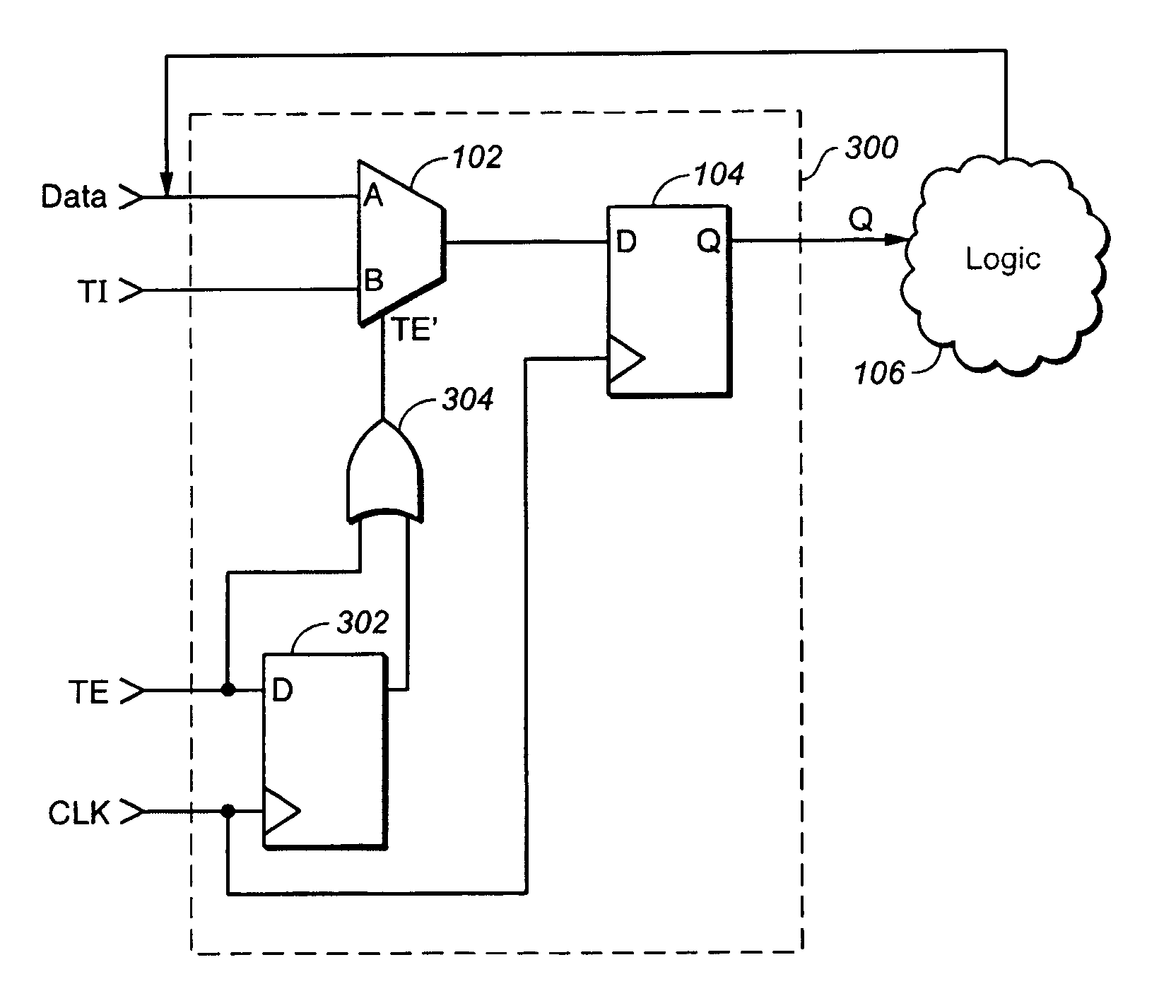
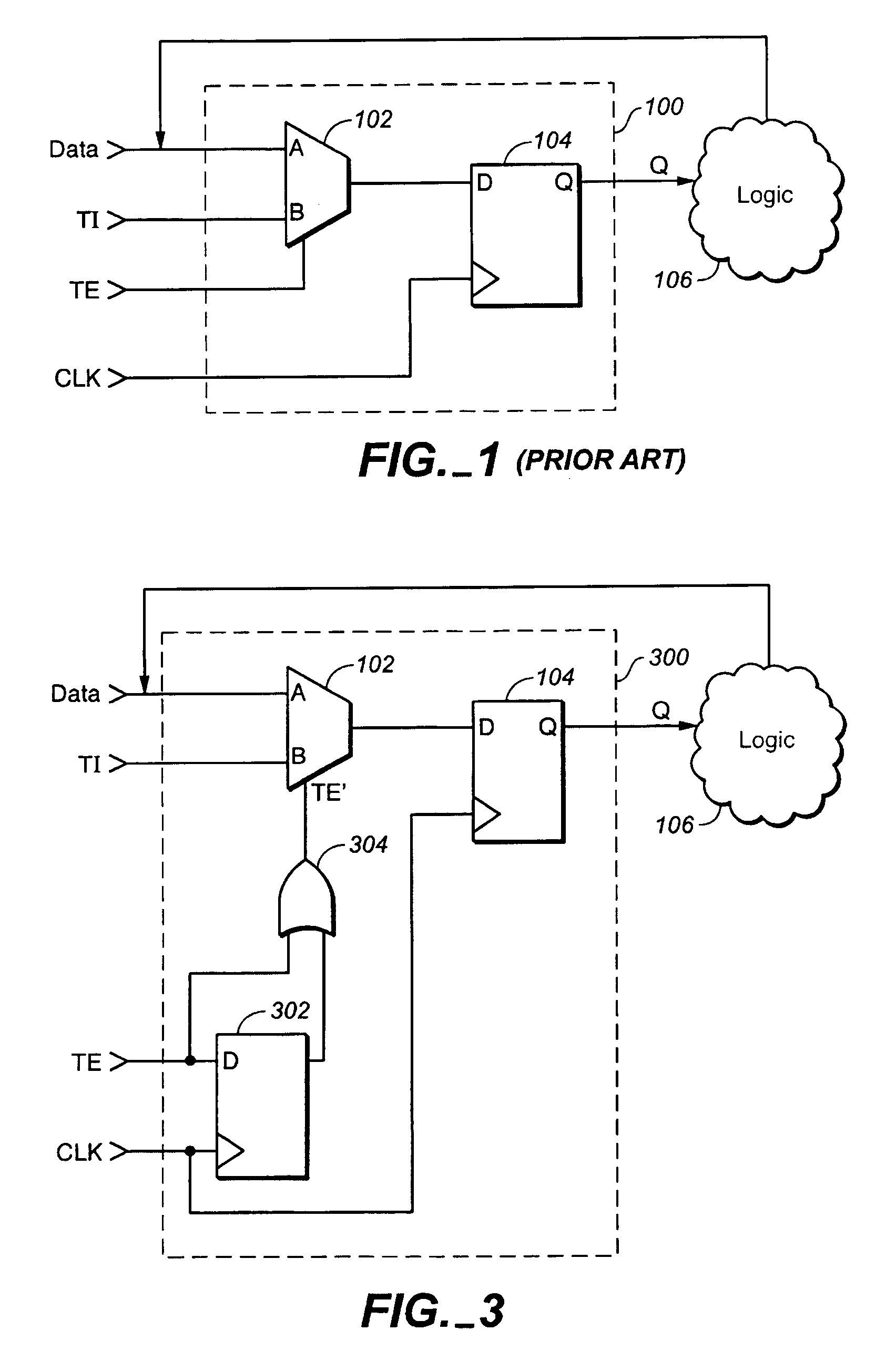
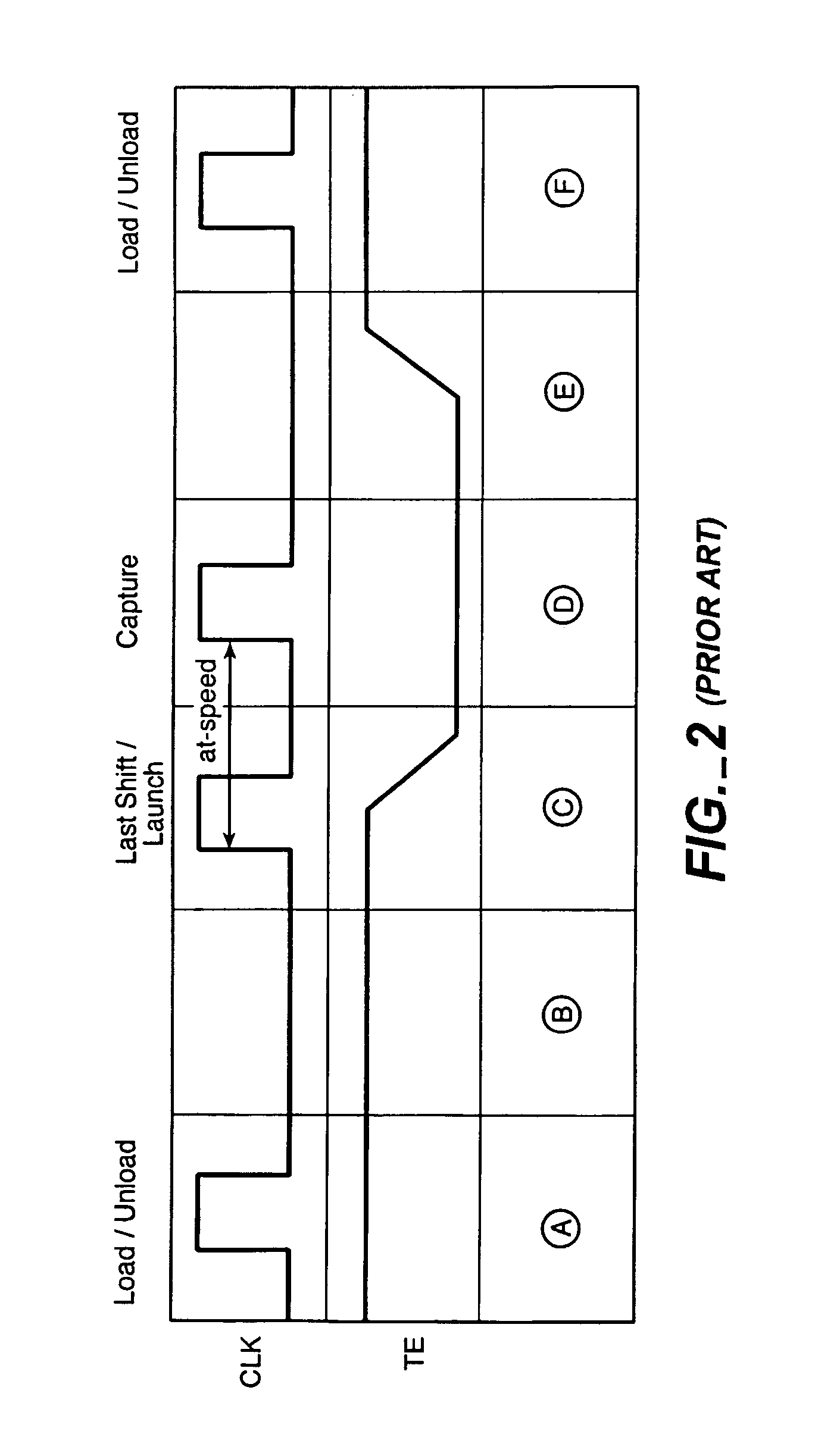
[0025]Delay-related effects in random logic are becoming increasingly significant in the overall defect density in semiconductor manufacturing as a result of increased operating frequencies and increased backend metal layers. This trend in delay defect density creates an additional need to test for and reject die having an inadequate speed performance due to delay-related defects. Screening for delay defects has traditionally been done through at-speed functional testing of the die. However, due to an increased ratio of internal nodes to external control and observation points, that is, primary inputs and outputs of the die, it becomes increasingly difficult to create functional test patterns in a time and cost efficient manner. A commonly used method for increasing the test capability of complex integrated circuit designs uses scan chains.

[0026]Scan testing is an effective alternative to functional testing for delay-related defects. One form of scan testing is commonly known as the...


PUM


Abstract

A self-timed scan circuit includes a multiplexer for selecting either a data input or a test input in response to an internal test enable signal and for generating a multiplexed output; a latch coupled to the multiplexer for generating a latched output in response to a next clock pulse; and a timing control circuit for generating the internal test enable signal in response to a global test enable signal wherein the internal test enable signal is set to logic one when the global test enable signal is set to logic one and wherein the internal test enable signal is set to logic zero in response to the next clock pulse.

Description

BACKGROUND OF THE INVENTION[0001]1. Field of the Invention[0002]The present invention is directed to the testing of integrated circuit devices. More specifically, but without limitation thereto, the present invention is directed to a method of testing integrated circuits that include synchronously clocked elements.[0003]2. Description of Related Art[0004]Modern electronics systems have increased dramatically in circuit density. For example, the densities of integrated circuits have increased from a few hundred transistors per chip in the 1960's to several million transistors per chip in integrated circuits manufactured today. Integrated circuit packaging density has increased from the previous relatively low density dual in-line package (DIP) having a typical pin count of 8 to 40 pins and a pin spacing of 0.1 inch to the current fine-pitch technology (FPT), tape-automated bonding (TAB), and multi-chip modules (MCMs) that provide hundreds of pins in relatively small packages. Conduct...

Claims


Application Information

Patent Timeline
Patent Type & Authority Patents(United States)
IPC IPC(8): G01R31/3185
CPCG01R31/318536G01R31/318558G01R31/318594
Inventor BENWARE, ROBERT
Owner AVAGO TECH WIRELESS IP SINGAPORE PTE
Why Eureka
Try Eureka