Method of forming narrow trenches in semiconductor substrates

a technology of semiconductor substrates and narrow trenches, applied in semiconductor devices, electrical apparatus, transistors, etc., can solve the problems of increasing gate charges of trench mosfet devices, and achieve the effect of reducing gate charges

Inactive Publication Date: 2005-12-20
GEN SEMICON
View PDF14 Cites 10 Cited by
  • Summary
  • Abstract
  • Description
  • Claims
  • Application Information

AI Technical Summary

Benefits of technology

[0014]One advantage of the present invention is that trenches with narrow widths can be formed within a semiconductor substrate.
[0015]Another advantage of the present invention is that a trench MOSFET device can be formed with narrow trenches, and hence reduced gate charges.
[0016]Another advantage of the present invention is that trench masks can be formed having apertures that are smaller than those directly obtainable from photolithographic processing.
[0017]These and other embodiments and advantages of the present invention will become immediately apparent to those of ordinary skill in the art upon review of the detailed description and claims to follow.

Problems solved by technology

Unfortunately, the gate charges associated with trench MOSFET devices also increase when cell density is increased.

Method used


Image

  • Method of forming narrow trenches in semiconductor substrates
  • Method of forming narrow trenches in semiconductor substrates
  • Method of forming narrow trenches in semiconductor substrates

Examples


Embodiment Construction

[0022]The present invention now will be described more fully hereinafter with frequent reference to the accompanying drawings, in which preferred embodiments of the present invention are shown. This invention may, however, be embodied in different forms and should not be construed as limited to the embodiments set forth herein.

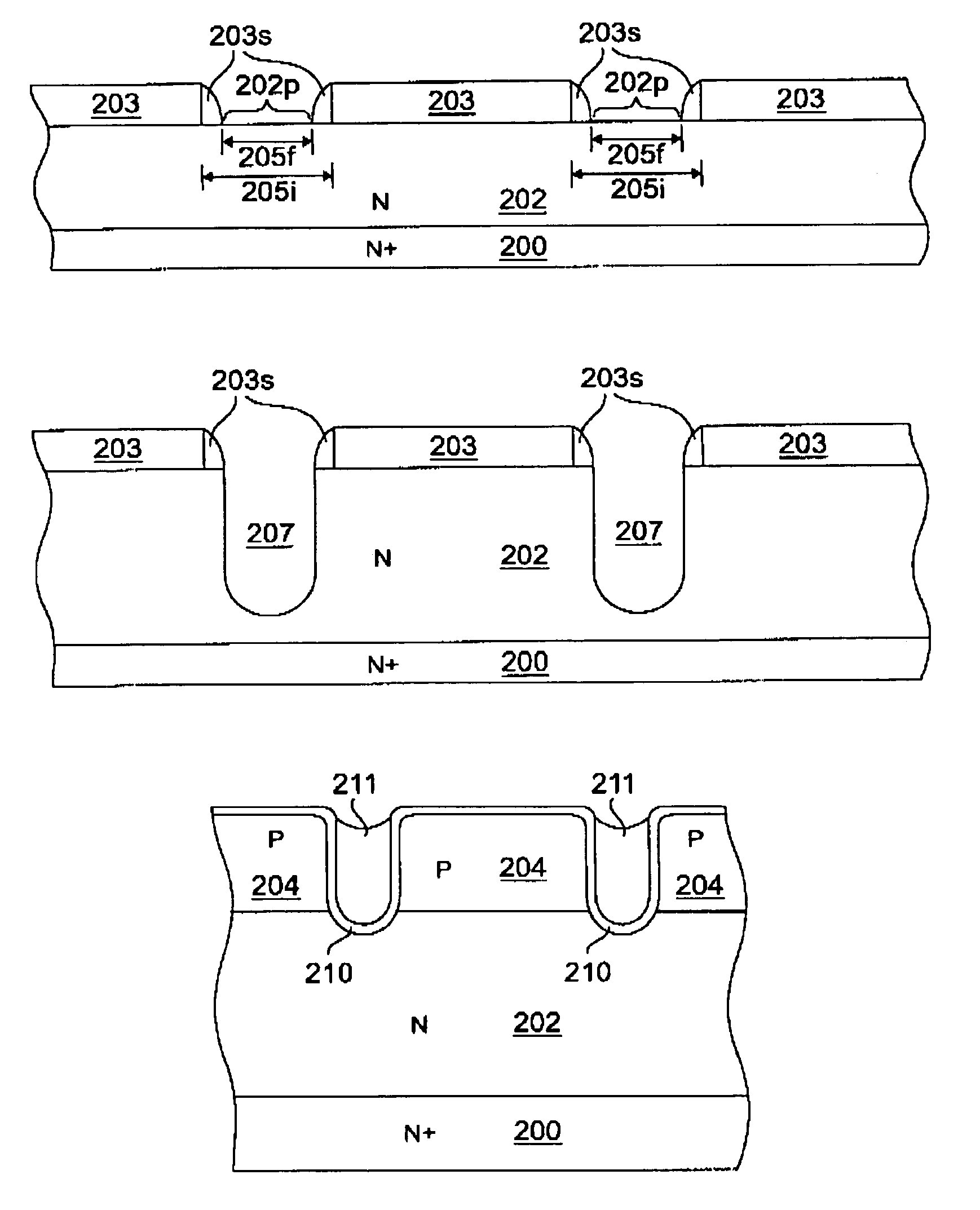
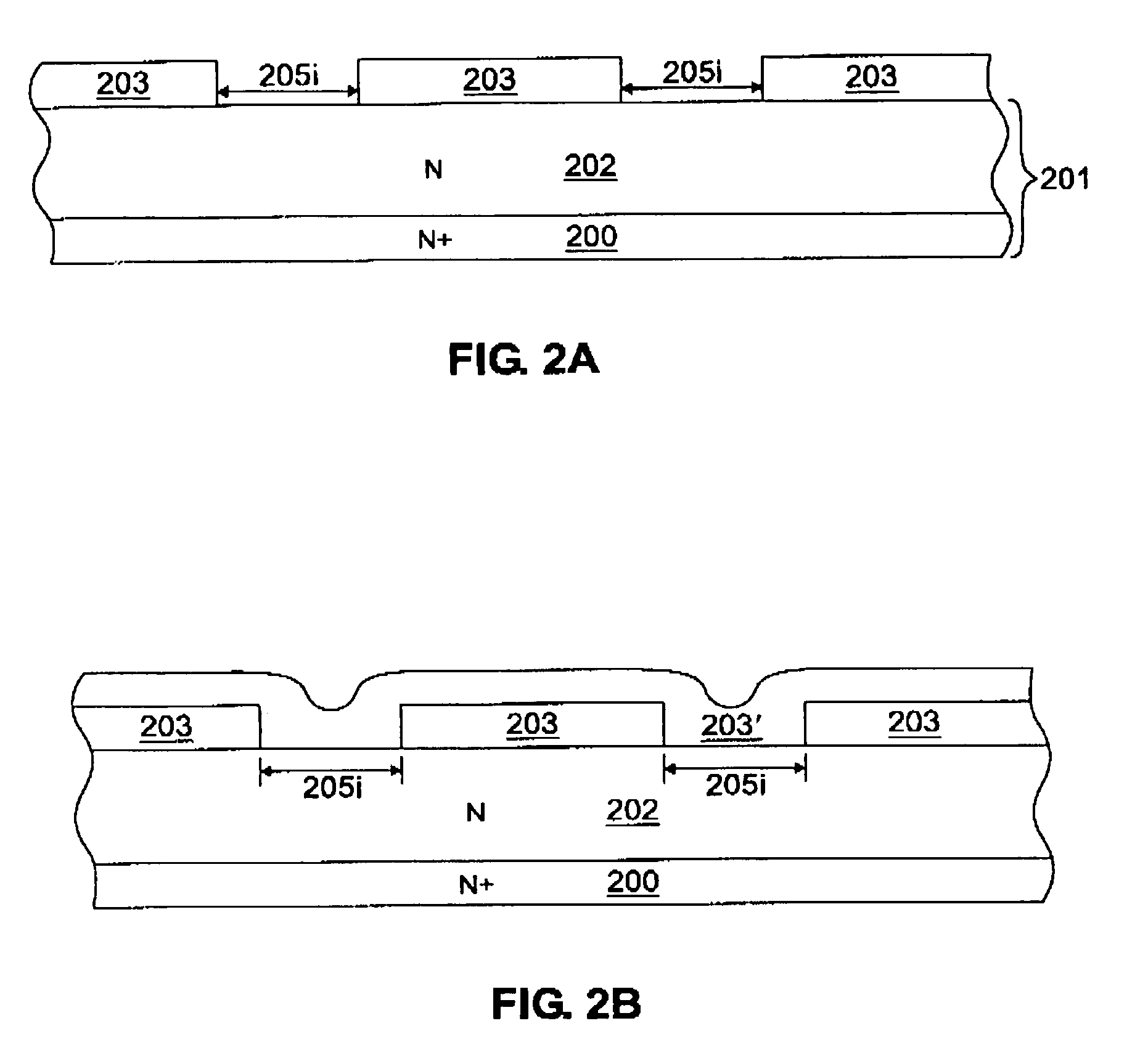
[0023]According to an embodiment of the present invention, a semiconductor substrate is the preferred substrate. The semiconductor substrate can be any such substrate known in the art, including elemental semiconductor substrates, such as silicon or germanium, or compound semiconductor substrates, such as GaAs, AlAs, GaP, InP, GaAlAs, and so forth. The semiconductor substrate can be single crystal, polycrystalline and / or amorphous, and it can be doped or undoped. A specific example of a semiconductor substrate is presented in connection with FIGS. 2A through 2D. Referring to FIG. 2A, a silicon semiconductor substrate 201 is shown, which consists of an N+ doped...


PUM


Abstract

A method of forming a trench within a semiconductor substrate. The method comprises, for example, the following: (a) providing a semiconductor substrate; (b) providing a patterned first CVD-deposited masking material layer having a first aperture over the semiconductor substrate; (c) depositing a second CVD-deposited masking material layer over the first masking material layer; (d) etching the second masking material layer until a second aperture that is narrower than the first aperture is created in the second masking material within the first aperture; and (e) etching the semiconductor substrate through the second aperture such that a trench is formed in the semiconductor substrate. In preferred embodiments, the method of the present invention is used in the formation of trench MOSFET devices.

Description

FIELD OF THE INVENTION[0001]This invention relates to methods of forming narrow trenches in semiconductor substrates.BACKGROUND OF THE INVENTION[0002]Narrow trenches are commonly desired during fabrication of a wide array of semiconductor devices. Hence, although a specific example concerning the utility of narrow trenches is discussed below in connection with trench MOSFET devices, it is noted that narrow trenches have utility throughout the semiconductor field.[0003]A trench MOSFET (metal-oxide-semiconductor field-effect transistor) is a transistor in which the channel is formed vertically and the gate is formed in a trench extending between the source and drain. The trench, which is lined with a thin insulator layer such as an oxide layer and filled with a conductor such as polysilicon (i.e., polycrystalline silicon), allows less constricted current flow and thereby provides lower values of specific on-resistance. Examples of trench MOSFET transistors are disclosed, for example, ...

Claims


Application Information

Patent Timeline
Patent Type & Authority Patents(United States)
IPC IPC(8): H01L21/28H01L21/3065H01L21/308H01L21/336H01L21/8234H01L27/088H01L29/12H01L29/423H01L29/49H01L29/78
CPCH01L21/3086H01L21/3088H01L21/18
Inventor HSHIEH, FWU-IUANSO, KOON CHONGAMATO, JOHN E.PRATT, BRIAN D.
Owner GEN SEMICON
Why Eureka
Try Eureka