Dual damascene circuit with upper wiring and interconnect line positioned in regions formed as two layers including organic polymer layer and low-permittivity layer

a damascene circuit and interconnect line technology, applied in semiconductor devices, semiconductor/solid-state device details, electrical devices, etc., can solve the problems of poor corrosion resistance of copper, difficult to form the upper groove and the via hole to a good shape, and difficult to pattern itself, etc., to achieve good electrical characteristics, reduce the effect of effective permittivity, and good shap

Inactive Publication Date: 2005-12-20
RENESAS ELECTRONICS CORP
View PDF20 Cites 5 Cited by
  • Summary
  • Abstract
  • Description
  • Claims
  • Application Information

AI Technical Summary

Benefits of technology

[0025]It is an object of the present invention to provide an integrated circuit device having upper wiring and an interconnect line formed to a go

Problems solved by technology

However, the properties of copper make it difficult to pattern itself by way of etching, and the corrosion resistance of copper is poor.
However, as the upper groove and the via hole are simultaneously formed in the single-layer upper interlayer film, it is difficult to form the upper groove and the via hole to a good shape, and it is particularly difficult to form the upper groove to a desired depth due to mircroloading.
However, as the upper groove and the via hole are simultaneously formed in the single-layer upper interlayer film, it is difficul

Method used


Image

  • Dual damascene circuit with upper wiring and interconnect line positioned in regions formed as two layers including organic polymer layer and low-permittivity layer
  • Dual damascene circuit with upper wiring and interconnect line positioned in regions formed as two layers including organic polymer layer and low-permittivity layer
  • Dual damascene circuit with upper wiring and interconnect line positioned in regions formed as two layers including organic polymer layer and low-permittivity layer

Examples


Embodiment Construction

[0046]An embodiment of the present invention will be described below with reference to FIG. 2 through FIG. 5c.

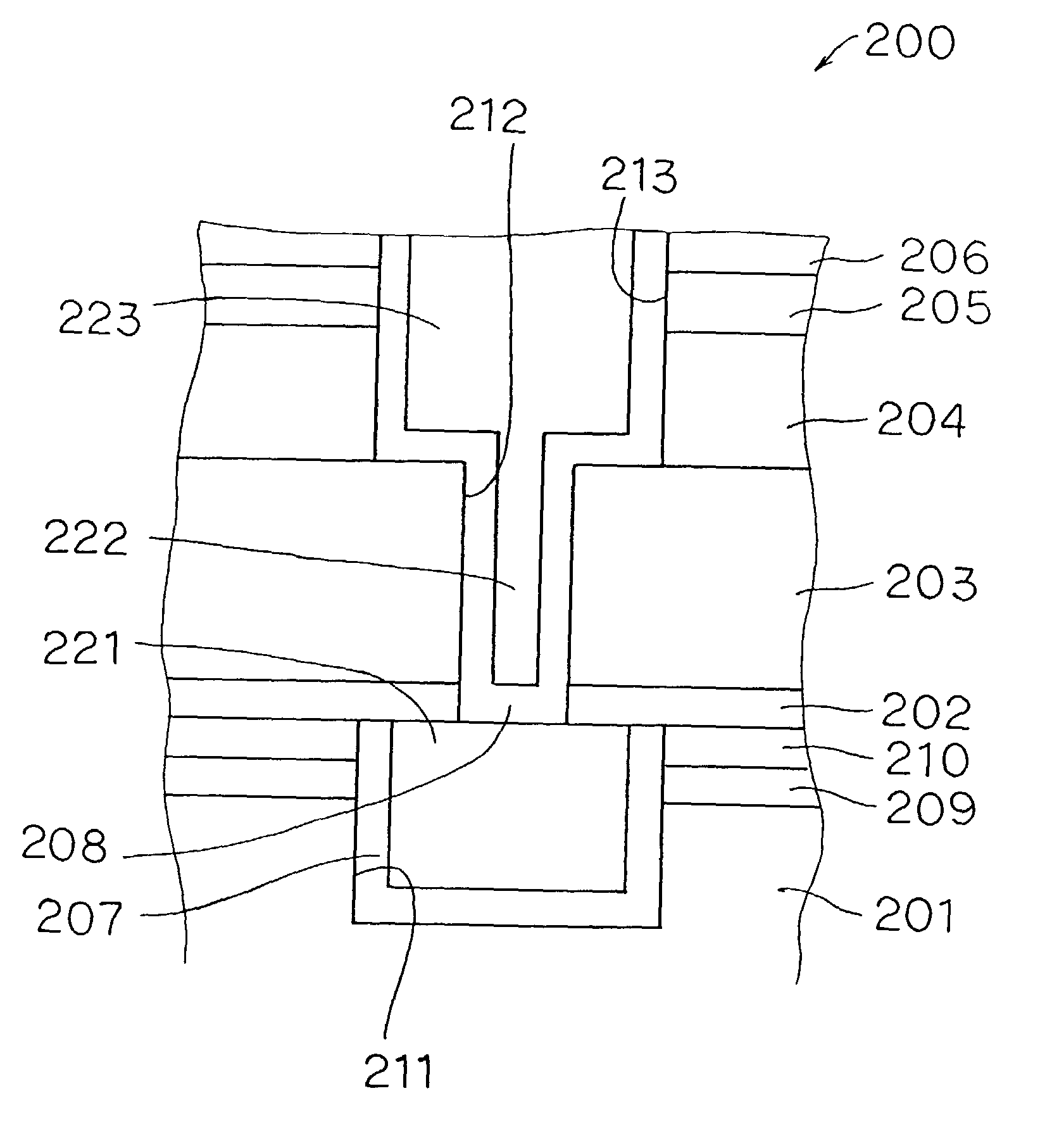
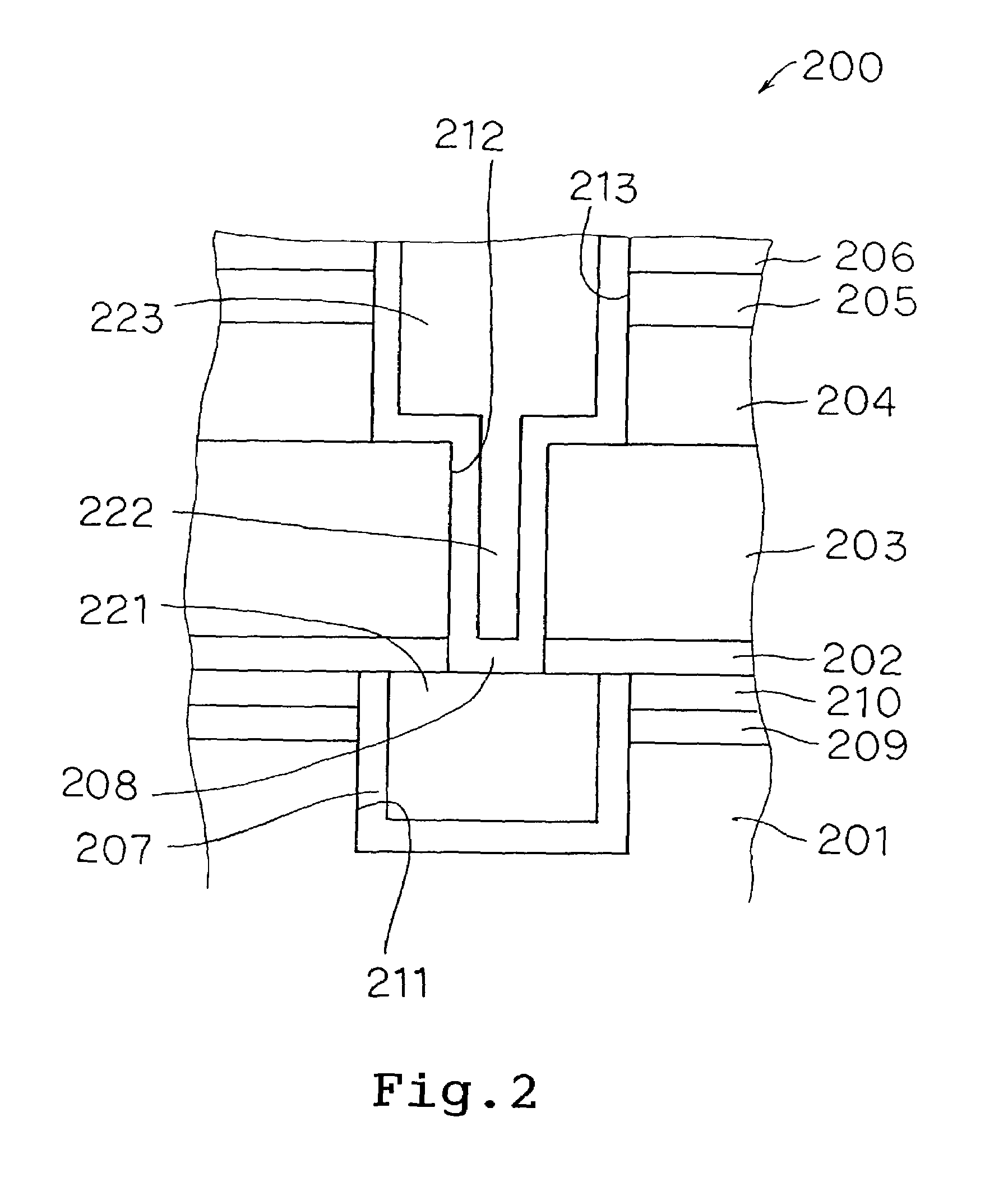
[0047]As shown in FIG. 2, dual damascene circuit 200 as an integrated circuit device according to an embodiment of the present invention has lower interlayer film 201 on which there are successively deposited barrier insulating film 202, organic polymer layer 203, low-permittivity layer 204, first mask layer 205, and second mask layer 206.

[0048]Lower groove 211 having a width of 0.4 μm is formed in lower interlayer film 201 from its upper surface to a certain depth. Lower wiring 221 is embedded in lower groove 211 with a metal barrier 207 interposed between lower wiring 221 and the wall of lower groove 211. Metal barrier 207 has a thickness of 300 Å and is made of TaN, and lower wiring 221 is made of Cu.

[0049]Barrier insulating film 202 has a thickness of 500 Å and is made of P—SiC. Barrier insulating film 202 is formed on the upper surface of lower interlayer film 201 and ...


PUM


Abstract

A dual damascene circuit has lower wiring and upper wiring positioned in regions formed as two layers including a CH-based organic polymer layer and a low-permittivity layer made of porous MSQ or the like. The organic polymer layer and the low-permittivity layer have high etching selectively with respect to each other to form an upper groove and a via hole to a good shape, allowing upper wiring and the interconnect line to have good electric characteristics. The organic polymer layer and the low-permittivity layer are low in density and permittivity, thus reducing the effective permittivity of the dual damascene circuit in its entirety.

Description

BACKGROUND OF THE INVENTION[0001]1. Field of the Invention[0002]The present invention relates to an integrated circuit device having lower wiring and upper wiring connected to each other by an interconnect line, and more particularly to an integrated circuit device fabricated according to the dual damascene process.[0003]2. Description of the Related Art[0004]To meet present demands for integrated circuits of higher performance and smaller patterns, there have been studied various processes for fabricating such integrated circuits and materials to be used in such integrated circuits. For example, while polysilicon or aluminum has heretofore been widely used as the wiring material in integrated circuits, a material having a lower resistance is required to achieve higher performance and smaller patterns for integrated circuits.[0005]It has been proposed to make fine wiring in integrated circuits of copper. However, the properties of copper make it difficult to pattern itself by way of...

Claims


Application Information

Patent Timeline
IPC IPC(8): H01L21/312H01L21/316H01L21/768H01L23/532
CPCH01L21/76811H01L21/76835H01L23/53238H01L23/53295H01L21/3124H01L21/31633H01L2924/0002H01L2924/00H01L21/768
Inventor USAMI, TATSUYA
Owner RENESAS ELECTRONICS CORP
Why Eureka
Try Eureka