Image display device

a display device and image technology, applied in the field of image display devices, can solve the problems of large power consumption, inability to completely neutralize charges, increase the area of the ic chip for the data driver, etc., and achieve the effect of simple structur

Inactive Publication Date: 2005-12-20
SHARP KK
View PDF8 Cites 25 Cited by
  • Summary
  • Abstract
  • Description
  • Claims
  • Application Information

AI Technical Summary

Benefits of technology

[0009]It is therefore an object of the present invention to realize an image display device suited for a large-size screen with a data signal line driving circuit of a simple structure.

Problems solved by technology

In the AC driving, however, when reversing polarities of voltages for gradation display, it is required for a data signal line driving circuit to charge them to a voltage for gradation display as desired after discharging a data signal line and a pixel capacitor by inputting charges in reverse polarity, which results in large amount of power consumption.
In the foregoing conventional techniques, it is required to provide a large number of output terminals in the data driver 1, and also to provide short-circuit switches sw1 to s2n in the data driver 1 besides the separation switches s1 to sn, which results in another problem of increasing an area of an IC chip for the data driver 1.
Therefore, it is more likely that charges cannot be neutralized completely due to a drop in voltage caused by a large wiring resistance, and the power consumption cannot be reduced significantly.

Method used


Image

  • Image display device
  • Image display device
  • Image display device

Examples


Embodiment Construction

[0058]The following will explain one embodiment of the present invention in reference to FIG. 1 through FIG. 11.

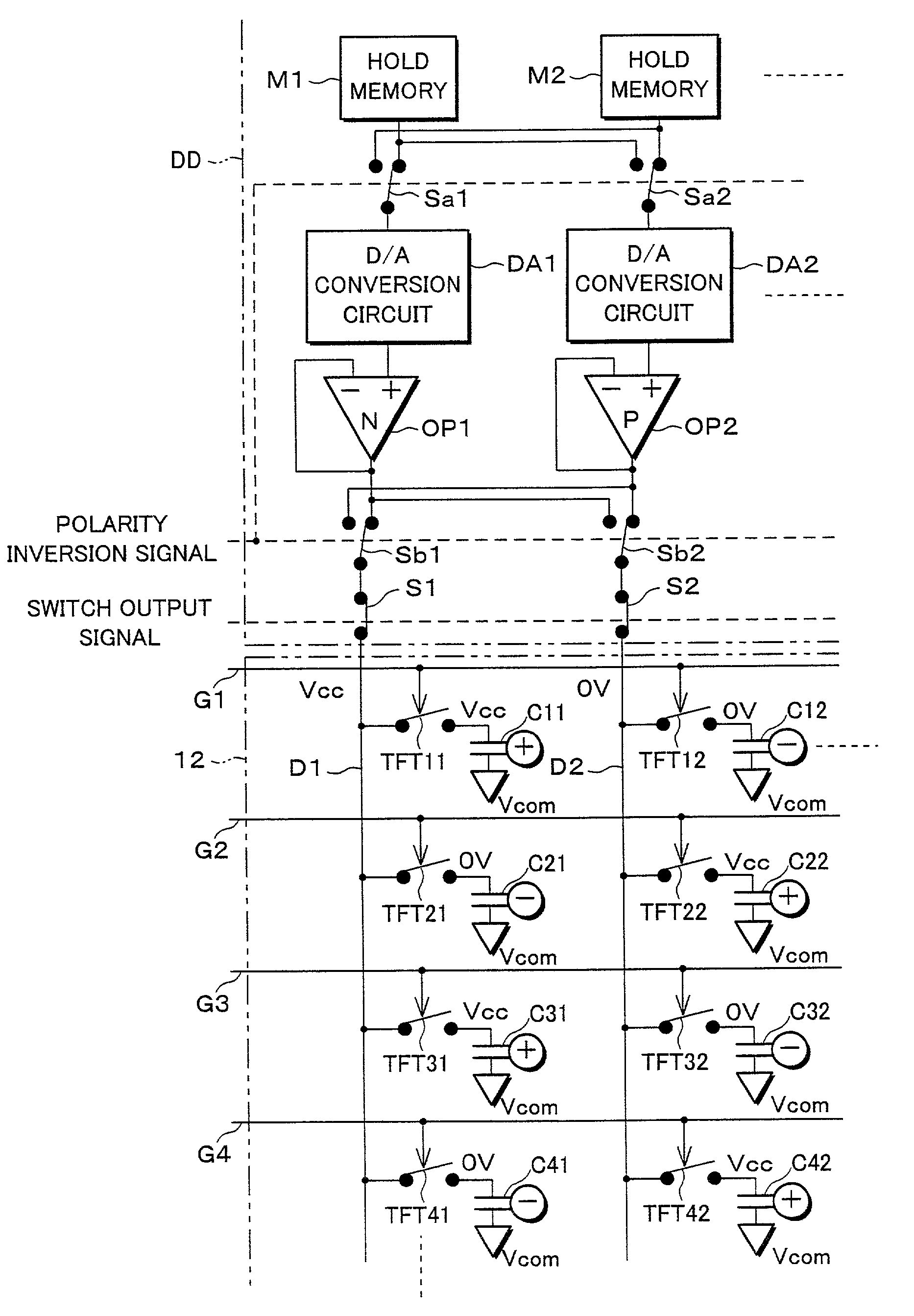
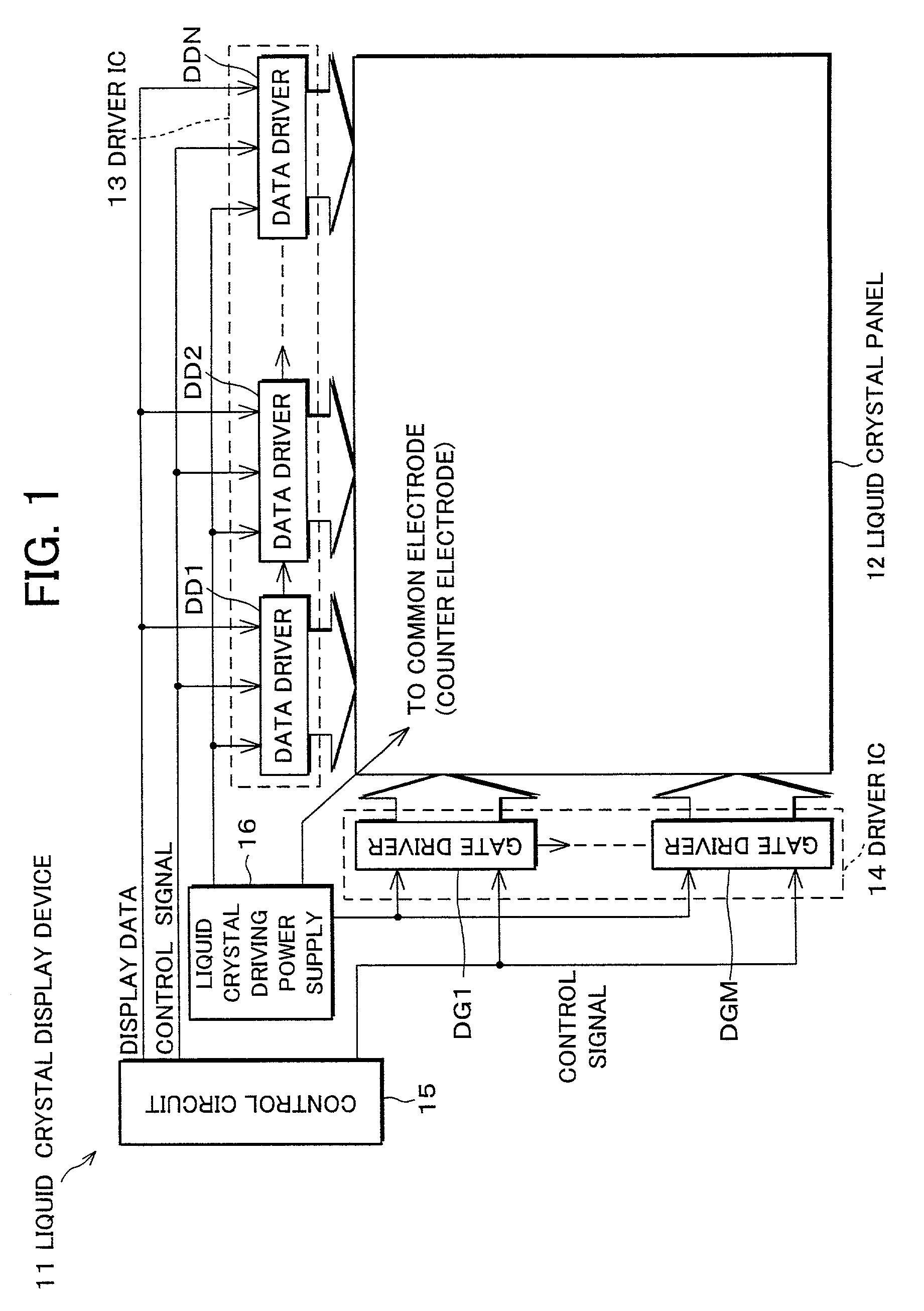
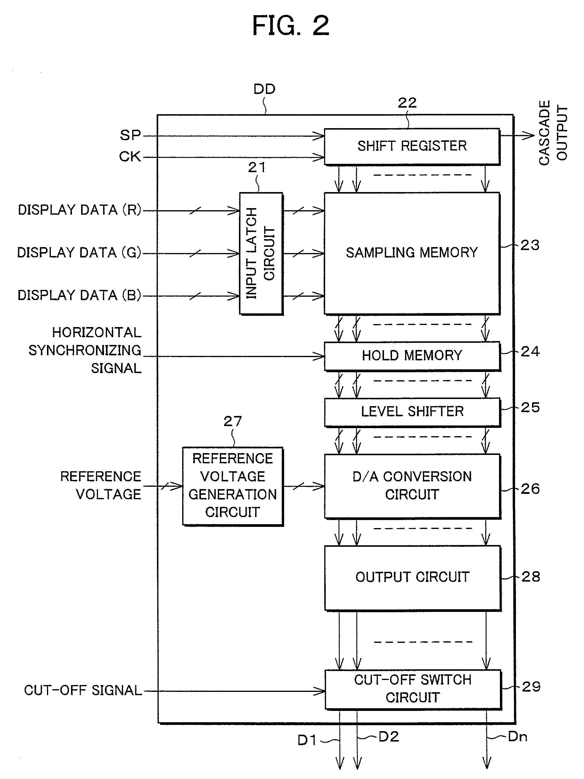
[0059]FIG. 1 is a block diagram illustrating an entire structure of a liquid crystal display device 11 in accordance with one embodiment of the present invention. As illustrated in FIG. 1, the liquid crystal display device 11 includes a liquid crystal panel 12 of the TFT active matrix type, and a driver IC 13 provided on one side of the liquid crystal panel 12, and a driver IC 14 provided on the other side of the liquid crystal panel 12. These driver ICs 13 and 14 selectively apply voltages from a liquid crystal driving power supply 16 to the liquid crystal panel 12 in response to outputs from a control circuit 15, to perform display operations. The driver IC 13 is composed of data drivers N in number, i.e., DD1 to DDN (hereinafter simply referred to as DD when it is not necessarily be specified), and the driver ID 14 is composed of gate drivers M in number, i.e., DG1 to D...


PUM

PropertyMeasurementUnit
threshold voltageaaaaaaaaaa
voltageaaaaaaaaaa
negative voltageaaaaaaaaaa

Abstract

A line inverse driving method is performed by outputting voltages for gradation display in mutually reverse polarities with respect to pixels adjacent in a data signal line direction. A separation switch is provided between an output stage of a data driver and a data signal line to separate them. In a blanking period, the data signal line is cut off, and in the selection-scanning period of a scanning signal line to be scanned first, the scanning signal line to be scanned next is also subjected to the selection-scanning. With this structure, respective charges in adjacent pixel capacitors are neutralized, and it is therefore possible to reduce a power consumption. Further, since a short-circuit can be performed at short distance, the problem of dull waveform can be suppressed, thereby realizing an image display device suited for a large screen.

Description

FIELD OF THE INVENTION[0001]The present invention relates to an image display device of the active matrix type including an electro-optical element, and a switching element and a pixel capacitor corresponding to the switching element provided in each pixel region surrounded by respective adjacent two lines of a plurality of scanning signal lines and a plurality of data signal lines which cross each other.BACKGROUND OF THE INVENTION[0002]For liquid crystal display devices or other similar devices, the AC driving is conventionally adopted to suppress deteriorations of liquid crystal elements (electro-optical elements). In the AC driving, however, when reversing polarities of voltages for gradation display, it is required for a data signal line driving circuit to charge them to a voltage for gradation display as desired after discharging a data signal line and a pixel capacitor by inputting charges in reverse polarity, which results in large amount of power consumption. As a typical co...

Claims


Application Information

Patent Timeline
Patent Type & Authority Patents(United States)
IPC IPC(8): G02F1/133G09G3/20G09G3/36
CPCG09G3/3614G09G3/3677G09G3/3688G09G2310/0251G09G2310/027G09G2310/0297G09G2330/023G09G3/36
Inventor OGAWA, YOSHINORIKATSUTANI, MASAFUMI
Owner SHARP KK
Why Eureka
Try Eureka