Liquid crystal display
a liquid crystal display and display technology, applied in non-linear optics, instruments, optics, etc., can solve the problems of the biggest defect of the tn type lcd, the fatal defect of the tft-lcd, and the narrow viewing angle, so as to suppress the drop in transmittance and improve the response characteristics
- Summary
- Abstract
- Description
- Claims
- Application Information
AI Technical Summary
Benefits of technology
Problems solved by technology
Method used
Image
Examples
first embodiment
[First Embodiment]
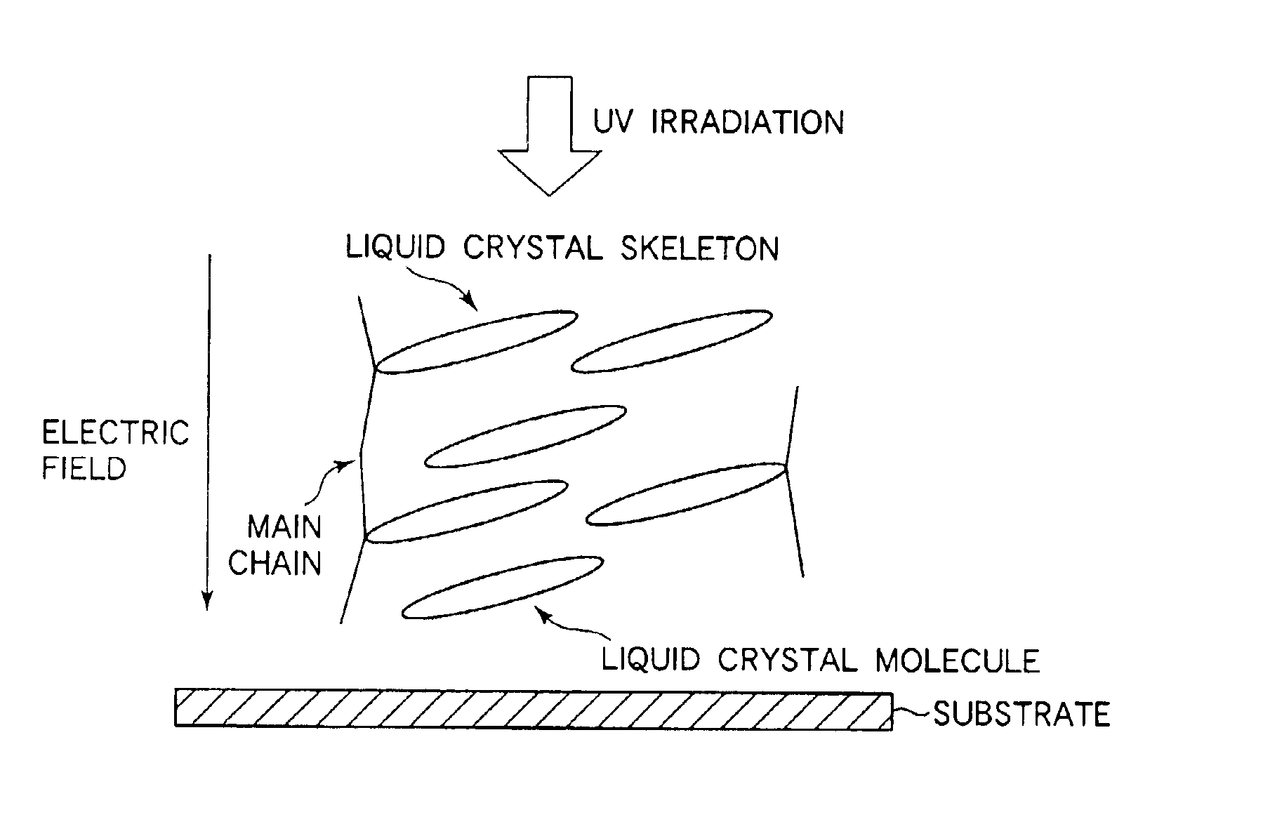
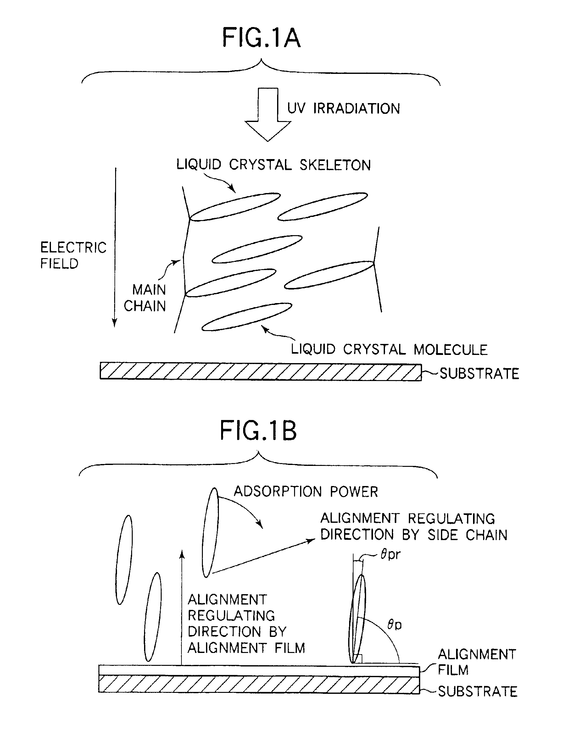
[0109]A liquid crystal display according to a first embodiment of the present invention will be described with reference to FIGS. 1A to 7. This embodiment is characterized in that in a liquid crystal display for regulating the alignment of all liquid crystal molecules at the time of voltage application by local alignment regulation, as typified by the above MVA system, a propagation process of a tilt of the liquid crystal molecule at the time of a response operation by voltage application is eliminated, and the whole display region is tilted at the same time. In addition, there is provided a liquid crystal display showing very high-speed response characteristics in all gradations by improving the response property itself of the liquid crystal molecules to an electric field.
[0110]In order to improve the response speed in the MVA system or the like, it is indispensable that a time required for tilt propagation of liquid crystal molecules is made zero and the whole su...
example 1-1
[0130]Liquid crystal monoacrylate monomer UCL-001-K1 of 2.5 wt % of Dainippon Ink Co., Ltd was added to liquid crystal material A having a negative dielectric anisotropy, and after being injected into an MVA cell, it was cured by ultraviolet rays while a voltage of 5.0 V was applied. Here, polyamic-acid material X was used as a vertical alignment film, banks (projections) each having a height of 1.5 μm and a width of 10 μm are alternately provided with resist LC-200 of Shipley Co., Ltd to make a space of 37.5 μm, and a cell gap was made 4.0 μm. A driving mode is normally-black.
[0131]FIG. 3 shows measurement results of response speed in this example. The horizontal axis indicates the transmittance (%) obtained when a predetermined voltage is applied from an applied voltage of 0 V, and the vertical axis indicates the response speed (ms; millisecond). A polygonal line α indicates a case where a photo-curing material is not added in the liquid crystal, and a polygonal line β indicates a...
example 1-2
[0134]In the MVA cell of the example 1-1, when the alignment state at the time of voltage application of 5.0 V was observed, disturbance of alignment caused by singular points generated on the alignment regulating structural members as shown in FIG. 75 was observed in the space portion between the alignment regulating structural members. When the change of the alignment state with respect to the applied voltage at the time of photo-curing was examined, an excellent alignment was obtained till application of 3V, and the disturbance of the alignment became noticeable from the time of application of 3.5 V.
[0135]Next, the alignment film material was changed to a polyamic-acid material whose vertical alignment ability is much stronger than that of vertical alignment film material X. and when a similar experiment was carried out, an excellent alignment was obtained till application of 3.5 V.
[0136]FIG. 5 shows the relation between the tilt angle of liquid crystal molecules on the alignment...
PUM
| Property | Measurement | Unit |
|---|---|---|
| tilt angle | aaaaa | aaaaa |
| twist angle | aaaaa | aaaaa |
| angle | aaaaa | aaaaa |
Abstract
Description
Claims
Application Information


