Manufacturing method for a semiconductor device using a marker on an amorphous semiconductor film to selectively crystallize a region with a laser light
a manufacturing method and semiconductor technology, applied in semiconductor devices, semiconductor/solid-state device details, electrical devices, etc., can solve the problems of reducing the current transportation characteristics of carriers, reducing the position and the size of crystal grains to form tft, and increasing the off current in tft, etc., to achieve the effect of increasing the processing efficiency of substrates, increasing processing speed, and large crystallization area
- Summary
- Abstract
- Description
- Claims
- Application Information
AI Technical Summary
Benefits of technology
Problems solved by technology
Method used
Image

Examples
embodiment 1
[0071]In this embodiment, a description will be given of a manufacturing method for an active matrix substrate with reference to FIGS. 6A to 9. Here, a substrate on which a CMOS circuit, a driver circuit, and a pixel portion having a pixel TFT and a storage capacitor are all formed is called an active matrix substrate for the sake of convenience.
[0072]First, in this embodiment, a substrate 600 made of glass such as barium borosilicate glass or alumino borosilicate glass is used. Further, as the substrate 600, a quartz substrate or a silicon substrate, or a metal substrate or a stainless steel substrate whose surface is covered with an insulating film may be used. Alternatively, a plastic substrate having a heat resistance to a processing temperature of this embodiment may be used.
[0073]Subsequently, on the substrate 600, a base film 601 made of an insulating film such as a silicon oxide film, a silicon nitride film, or a silicon oxynitride film is formed using a known method (sputte...
embodiment 2
[0111]This embodiment shows an embodiment in a case of including a step of crystallizing a semiconductor film using a catalyst. Here, only a point different from Embodiment 1 will be shown. When a catalytic element is used, it is desirable to employ the techniques disclosed in JP 7-130652 A and JP 8-078329 A.
[0112]After being formed, the amorphous semiconductor film is subjected to solid phase crystallization using Ni. For example, when the technique disclosed in JP 7-130652 A is used, a nickel acetate solution containing 10 ppm of nickel in terms of weight is applied onto the amorphous semiconductor film to form a layer containing nickel. After a dehydrogenation step at 500° C. for 1 hour, heat treatment at 500 to 650° C. for 4 to 12 hours, for example, heat treatment at 550° C. for 8 hours is performed to achieve crystallization. Note that, as a usable catalytic element, the following elements may be used in addition to nickel (Ni), that is, germanium (Ge), iron (Fe), palladium (P...
embodiment 3
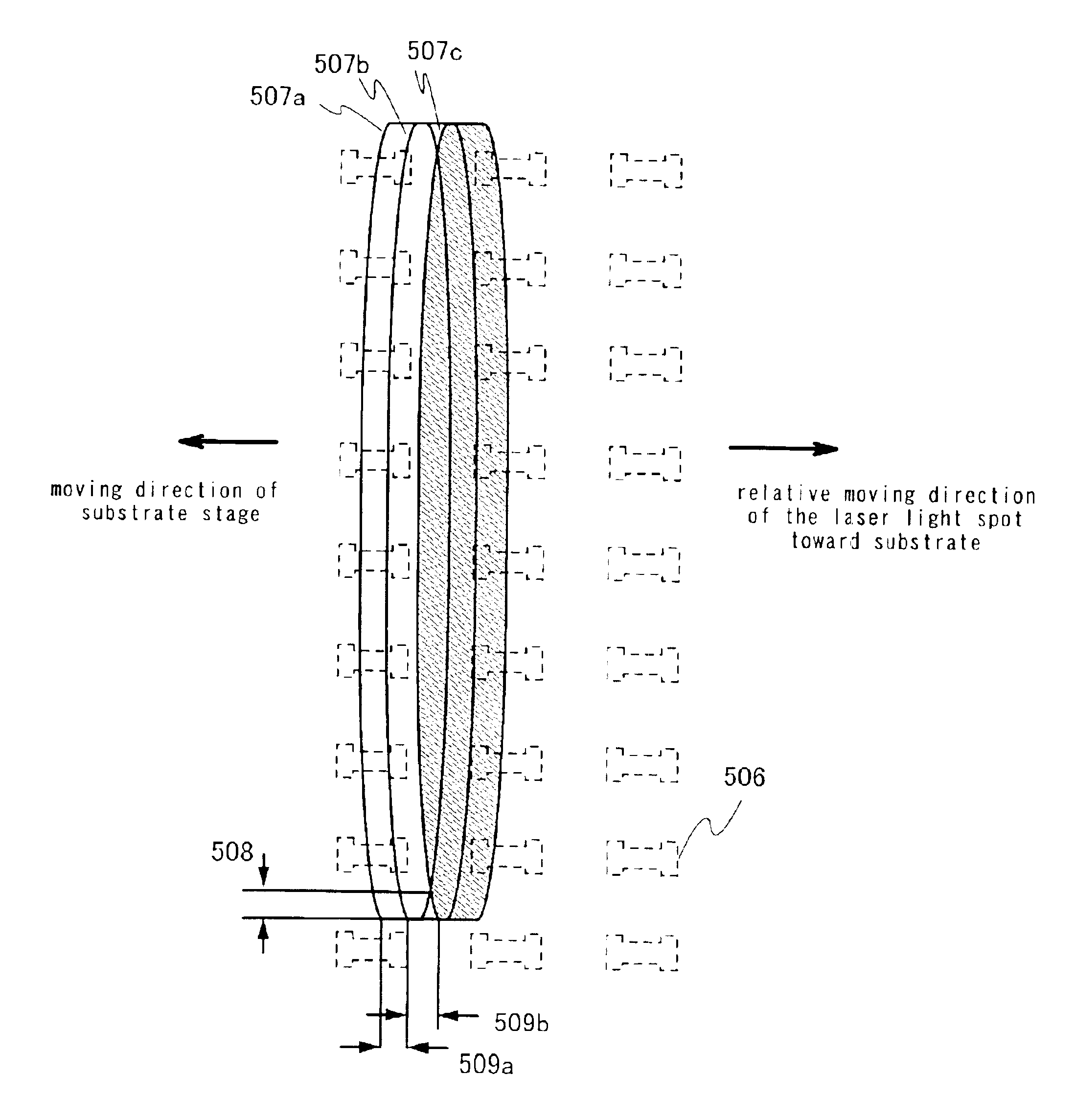
[0115]In this embodiment, an example of markers formed in a marker formation portion 423 will be shown. This embodiment can be implemented in combination with Embodiment 1 or 2.
[0116]FIG. 12A is a top view showing the markers of this embodiment. Reference numerals 421 and 422 denote markers formed in the semiconductor film as a reference (hereinafter, referred to as reference markers), which each have a rectangular shape. The reference markers 421 are arranged such that longer sides of the rectangle are disposed in a horizontal direction in all the markers. The respective reference markers 421 are arranged in a vertical direction at a regular interval. The reference markers 422 are arranged such that longer sides of the rectangle are disposed in a vertical direction in all the markers. The respective reference markers 422 are arranged in a horizontal direction at a regular interval.
[0117]The reference markers 421 are used as a reference for positioning the masks in the vertical dire...
PUM
| Property | Measurement | Unit |
|---|---|---|
| distance | aaaaa | aaaaa |
| distance | aaaaa | aaaaa |
| wavelength | aaaaa | aaaaa |
Abstract
Description
Claims
Application Information
 - R&D Engineer
- R&D Manager
- IP Professional
- Industry Leading Data Capabilities
- Powerful AI technology
- Patent DNA Extraction
Browse by: Latest US Patents, China's latest patents, Technical Efficacy Thesaurus, Application Domain, Technology Topic.
© 2024 PatSnap. All rights reserved.Legal|Privacy policy|Modern Slavery Act Transparency Statement|Sitemap