

LED drive circuit
a technology of led drive circuit and led drive, which is applied in the direction of pulse generator, pulse technique, instruments, etc., can solve the problems of reducing the luminance of led, and achieve the effect of reducing the power consumption of led drive circui
- Summary
- Abstract
- Description
- Claims
- Application Information
AI Technical Summary
Benefits of technology
Problems solved by technology
Method used
Image

Examples
embodiment 1
(Embodiment 1)
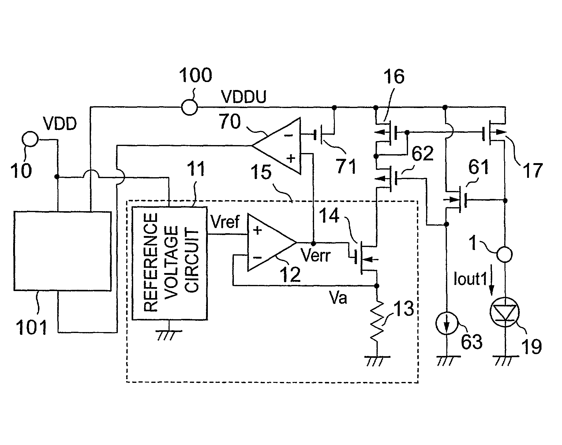
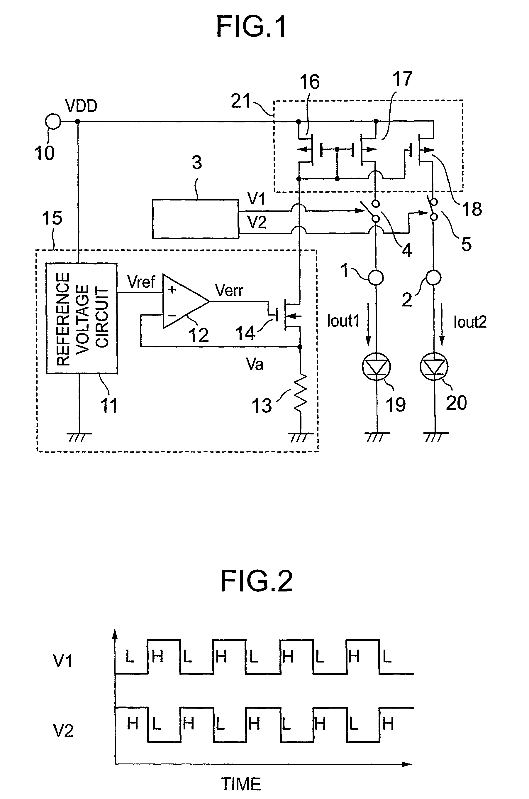
[0029]Embodiments of the present invention will be described with reference to the accompanying drawings. FIG. 1 shows an LED drive circuit which represents Embodiment 1 of the present invention. A constant current generation circuit 15, a current mirror circuit 21, and LEDs 19 and 20 shown in FIG. 1 are the same as those in the conventional arrangement.
[0030]Switches 4 and 5 are respectively inserted between transistors 17 and 18 in the current mirror circuit and terminals 1 and 2 to which the LEDs are connected. ON / OFF control of the switches 4 and 5 is performed by means of signal voltages V1 and V2 from a switch control circuit 3.
[0031]FIG. 2 shows an example of signal voltages V1 and V2 from the switch control circuit 3. The abscissa represents time and the ordinate comprises two components respectively representing voltages V1 and V2. In the example shown in FIG. 2, voltages V1 and V2 change in a complementary relationship with each other. When V1 is high level (...
embodiment 2
(Embodiment 2)
[0039]FIG. 4 shows an LED drive circuit which represents Embodiment 2 of the present invention. The same constant current generation circuit 15, current mirror circuit 21, and LEDs 19 and 20 as those in the conventional arrangement are used. Switches 4 and 5 are respectively inserted between transistors 17 and 18 in the current mirror circuit and terminals 1 and 2 to which the LEDs are connected. ON / OFF control of the switches 4 and 5 is performed by means of signal voltages V1 and V2 from a switch control circuit 6. A control terminal 7 to which a signal is externally supplied is connected to the switch control circuit 6. The cycle in which V1 and V2 change or the lighting time is controlled on the basis of signal V7 supplied through the control terminal 7.
[0040]FIGS. 5A and 5B show an example of a change in cycle. FIG. 5A shows a case where the voltage V7 on the control terminal 7 is low, and FIG. 5B shows a case where the voltage V7 on the control terminal 7 is high...
embodiment 3
(Embodiment 3)
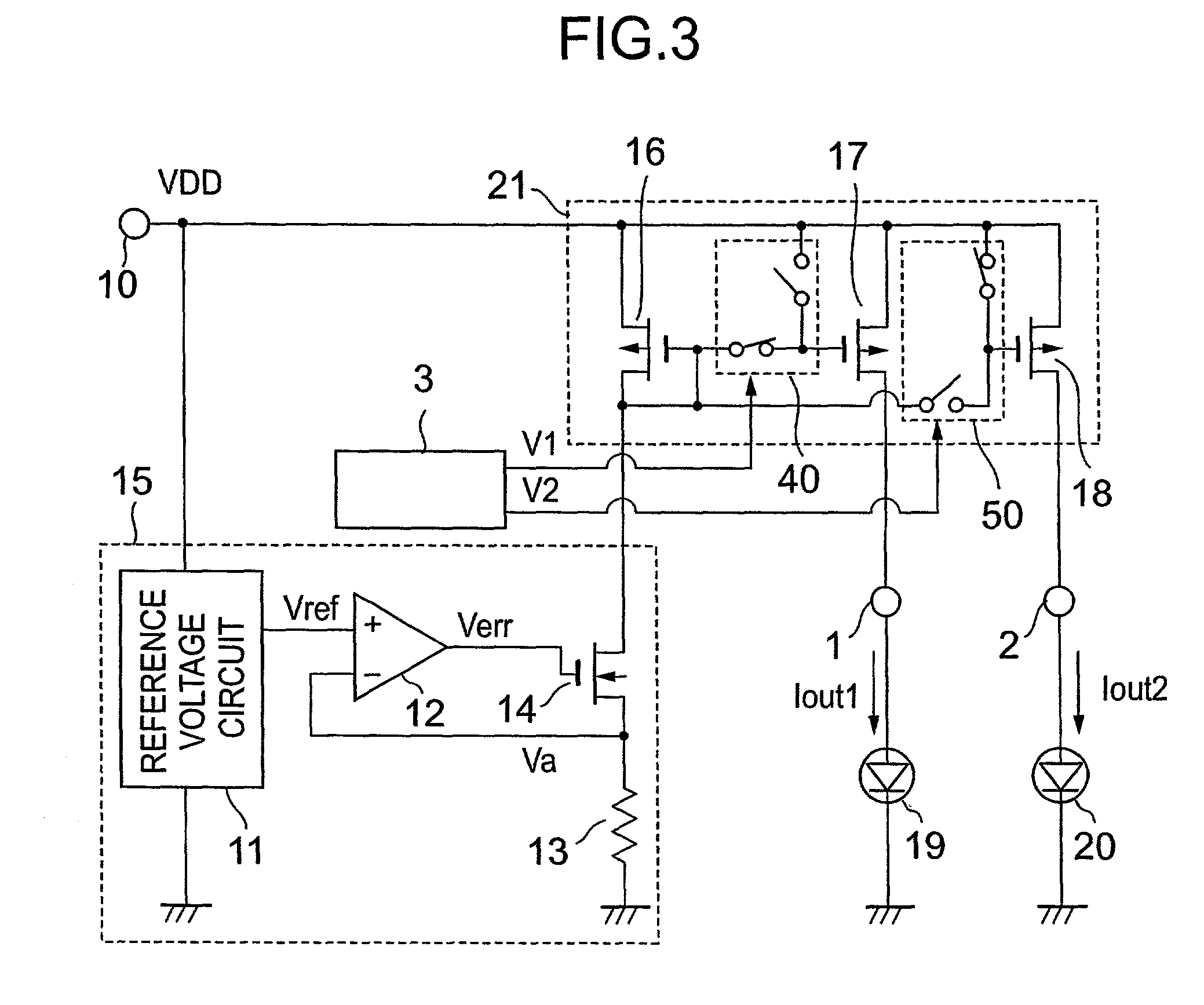
[0048]FIGS. 9A and 9B show Embodiment 3 of the present invention in which an LED is selected as an object of blinking control through a signal supplied to the control terminal 7 in the circuit shown in FIG. 3.
[0049]FIG. 9A shows voltages V1 and V2 when the voltage V7 on the control terminal 7 is low, and FIG. 9B shows voltages V1 and V2 when the voltage V7 on the control terminal 7 is high. When the voltage V7 on the control terminal 7 is low, the LED 19 is continuously lighted by maintaining V1 at H and control of blinking of the LED 20 is performed. On the other hand, when the voltage V7 on the control terminal 7 is high, the LED 20 is continuously lighted by maintaining V2 at H and control of blinking of the LED 19 is performed.
[0050]In Embodiment 3, one of a plurality of LEDs is continuously lighted while at least one of the other LEDs is controlled so as to blink, thus enabling LED drive for a backlight under a requirement of low power consumption according to use...
PUM
 Abstract
Description
Claims
Application Information