Micro-lens arrays for display intensity enhancement

a micro-lens array and display technology, applied in the field of organic light emitting devices and micro-lens arrays, can solve the problems that the current liquid crystal display technology used by most flat-panel displays is limited in its ability to meet these increasing demands, and achieve the effect of enhancing the light coupling efficiency of light emitting devices

Inactive Publication Date: 2006-01-10
THE TRUSTEES FOR PRINCETON UNIV
View PDF10 Cites 145 Cited by
  • Summary
  • Abstract
  • Description
  • Claims
  • Application Information

AI Technical Summary

Benefits of technology

[0011]The present invention is directed to micro-lens arrays for enhancing light coupling efficiency of light emitting devices containing OLEDs. In preferred embodiments, such a microlens array may include a plurality of microlenses. Each of the microlenses has a minimum planar dimension and a maximum planar dimension. The minimum planar dimensions of the microlenses are larger than the maximum wavelength of visible light emitted from the OLEDs. The maximum planar dimensions of the microlenses are smaller than the smallest minimum planar dimension of any of the plurality of OLEDs.

Problems solved by technology

The display device of choice for such applications is a flat-panel display, but the current liquid crystal display (LCD) technology in use by most flat-panel displays is limited in its ability to meet these increasing demands.
One limitation of an un-doped device is that the multifunctional layer 113′ must have good electron transport capability.

Method used


Image

  • Micro-lens arrays for display intensity enhancement
  • Micro-lens arrays for display intensity enhancement
  • Micro-lens arrays for display intensity enhancement

Examples


Embodiment Construction

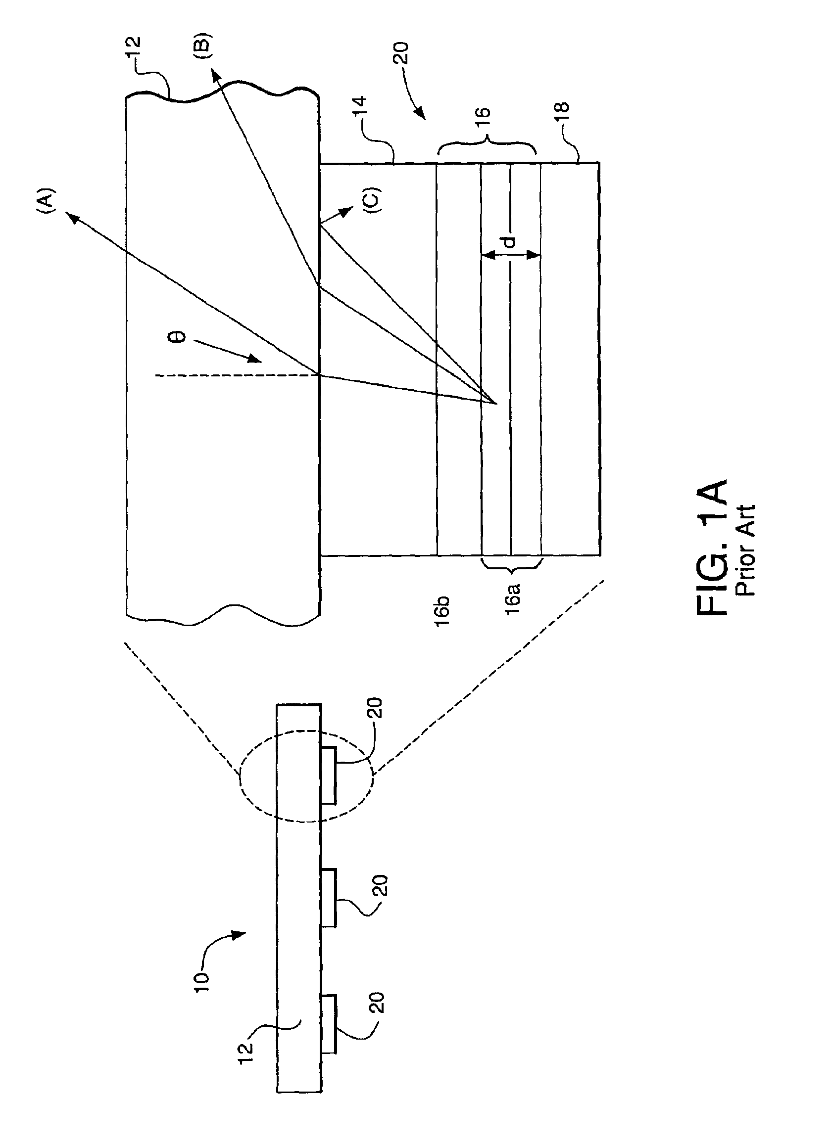
[0028]A light emitting device according to the invention can include, as shown in FIG. 2, a microlens substrate 102 and a plurality of organic light emitting devices (OLEDs) 20. Each OLED 20 can include an anode layer 14, at least one organic layer 16, and a reflecting cathode 18. The anode layer 14 is typically made of Indium Tin Oxide (ITO), and has a typical thickness, tITO, of about 150 nm and an index of refraction, nITO, of about 1.8. The organic layer 16 has a typical thickness, torg, of about 100 nm, and an index of refraction, norg, of between about 1.6 and 1.8. The cathode 18 is typically made of Mg:Ag, Li:Al, Li2O:Al, or LiF:Al. As shown, the device can include an electron transporting (ETL) and electroluminescent (EL) layer 16a of tris(8-hydroxyquinoline) aluminum (Alq3), with an index of refraction, nalq, of about 1.72. The device can include a hole transporting layer (HTL) 16b of 4, 4′-bis[N-(1-napthyl)-N-phenyl-amino] biphenyl (α-NPD), with an index of refraction, nNP...


PUM


Abstract

A microlens array for a light emitting device is disclosed. The light emitting device includes a plurality of OLEDs, each OLED having a minimum planar dimension. The array includes a plurality of microlenses, each of which has a minimum planar dimension and a maximum planar dimension. The minimum planar dimensions of the microlenses are larger than the maximum wavelength of visible light emitted from the OLEDs. The maximum planar dimensions of the microlenses are smaller than the smallest minimum planar dimension of any of the OLEDs.

Description

CROSS-REFERENCE TO RELATED APPLICATIONS[0001]This application claims priority from U.S. Provisional Patent Application Ser. No. 60 / 304,531, filed Jul. 10, 2001, the contents of which are incorporated herein by reference. This application claims priority from U.S. Provisional Patent Application Ser. No. 60 / 315,902, filed Aug. 30, 2001, the contents of which are incorporated herein by reference.FIELD OF THE INVENTION[0002]This invention relates generally to the field of light emitting devices, and more particularly to organic light emitting devices and microlens arrays for enhancing the coupling efficiency thereof.BACKGROUND OF THE INVENTION[0003]Access to the Internet and the need to download and view vast quantities of data at greater and greater speeds, along with a frequent requirement for portability and a small footprint are placing greater demands on the capabilities of display devices. The display device of choice for such applications is a flat-panel display, but the current ...

Claims


Application Information

Patent Timeline
Patent Type & Authority Patents(United States)
IPC IPC(8): H05B33/00G02B3/00H01L25/075H01L33/58
CPCG02B3/0031G02B3/0056H01L51/5275H01L33/58H01L25/0753H01L2924/0002H10K50/858H01L2924/00
Inventor MOLLER, SVENFORREST, STEPHEN R.
Owner THE TRUSTEES FOR PRINCETON UNIV
Why Eureka
Try Eureka