EMC shield and housing for electronic components

a technology of electronic components and shields, applied in the direction of electrical equipment, electrical apparatus, electrical apparatus construction details, etc., can solve the problems of lack of shielding between individual electronic components, large shielding housing, and large number of solder points, so as to improve the electrical contact, improve the shielding housing, and position the shield housing on the printed circuit board more easily and more accurately

Inactive Publication Date: 2006-01-10
SIEMENS AG
View PDF15 Cites 10 Cited by
  • Summary
  • Abstract
  • Description
  • Claims
  • Application Information

AI Technical Summary

Benefits of technology

[0009]In another preferred embodiment of the invention, the housing has at least one lug with a recess, in particular a hole for a screw to pass therethrough.
[0010]In order to improve the electrical contact between the housing and the printed circuit board, the printed circuit board may also have a solder deposit on its surface facing the housing.
[0011]The printed circuit board preferably has at least one recess for accommodating at least one shield housing projection, the projection being intended to engage the recess. Accordingly, it is possible to more easily and accurately position the shield housing on the printed circuit board.
[0012]In order to form an EMC shield for all sides of an electronic components, the layout of the printed circuit board may further comprise a surface or surface pattern which provides shielding against electromagnetic radiation for a component placed above or below the surface or surface portion. The housing may be a metal housing or a metalized plastic housing.
[0013]In another embodiment of the present invention, the present invention comprises an EMC housing for electromagnetic shielding of electronic components on a printe

Problems solved by technology

Such degradation would otherwise have resulted from electromagnetic interference.
A disadvantage to this approach is that the provision of connections which have to be passed out of the shielding housing from the printed circuit board in an EMC-compliant manner requires that there be a lack of shie

Method used


Image

  • EMC shield and housing for electronic components
  • EMC shield and housing for electronic components

Examples


Embodiment Construction

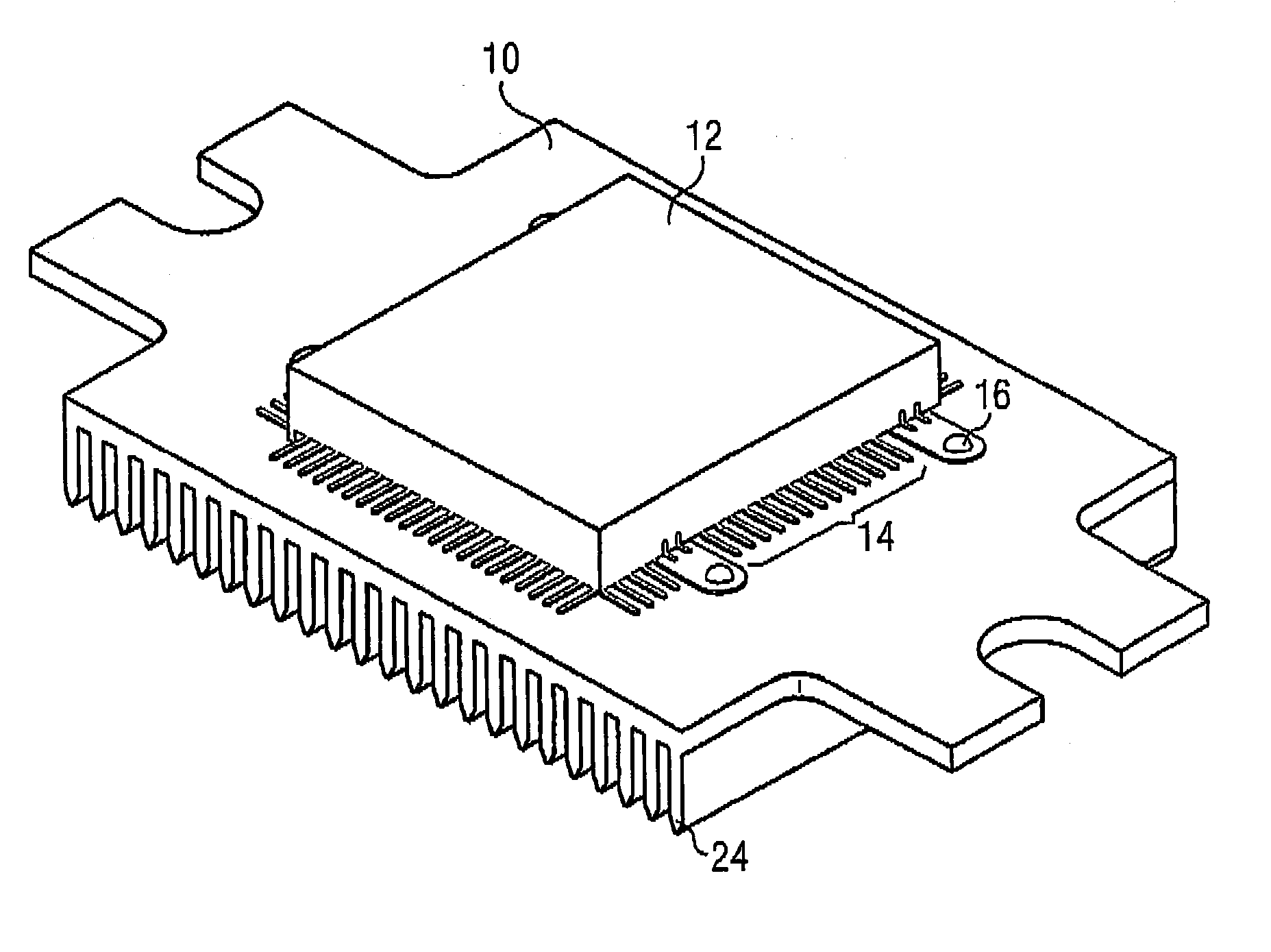
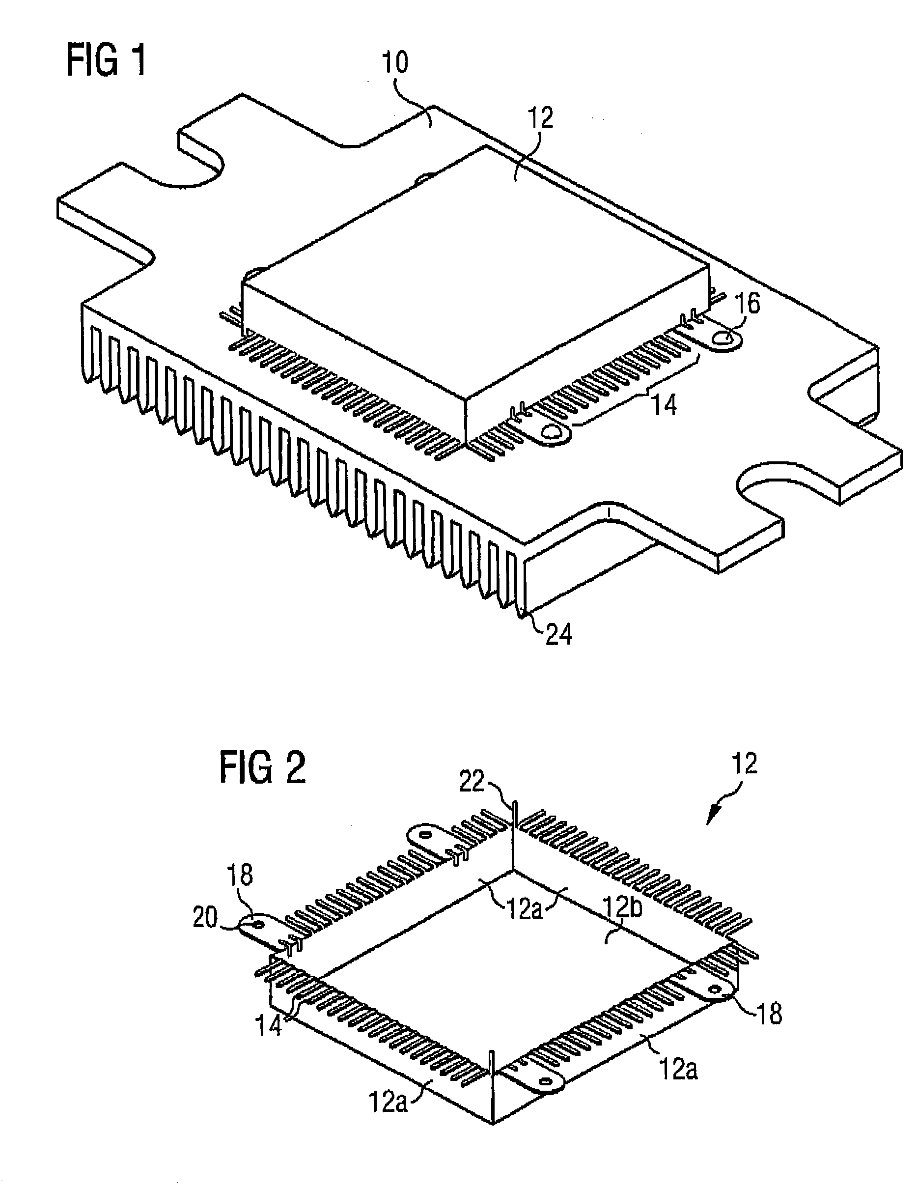
[0019]As may be seen from FIG. 1, the instant EMC shield shields components mounted on printed circuit board 10. The expression shielding will be used to mean not only the protection of the electronic components against external electromagnetic radiation but also the reduction of electromagnetic radiation produced by electronic components towards to components external to the shield.

[0020]The EMC shield comprises an EMC housing 12 having numerous side walls 12a and a cover 12b. In the depicted embodiment, cover 12b is rectangular therefore leading to four side walls 12a. Other cover configurations are possible leading to a different number of side walls. The present invention is not restricted by housing shape. Depending on the number, size and arrangement of the electronic components to be shielded on the printed circuit board 10, the housing 12 may also have only three or less or four or more side walls 12a and widely differing cover shapes 12b. The EMC shield housing 12 is prefer...


PUM


Abstract

An EMC shield is provided for electronic components on a printed circuit board, which has a housing which surrounds the electronic components at least on the sides not facing the printed circuit board and shields them against electromagnetic radiation, with the housing having a number of electrically conductive spring contacts which make electrically conductive contact with the printed circuit board, and the housing being pressed against the printed circuit board by means of at least one pressure contact-making device.

Description

CROSS REFERENCE TO RELATED APPLICATIONS[0001]The present application claims priority to German patent application number 10223170.2, filed May 24, 2002 which is herein incorporated by reference.BACKGROUND OF THE INVENTION[0002]The present invention relates to the field of radiation protection for printed circuit board components and more particularly to an electromagnetic compatability (EMC) shield and housing for such components. The instant shield and housing provide for the possibility for many different component to operate within a substantially electromagnetic environment without degradation in individual performance and the like. Such degradation would otherwise have resulted from electromagnetic interference.[0003]Shielding against electromagnetic radiation is becoming increasingly relevant for electronic apparatus as their sensitivity is becoming ever greater, their performance is increasing, and modern electronic components comprise ever higher clock rates. The EMC as defi...

Claims


Application Information

Patent Timeline
IPC IPC(8): H05K7/14H05K7/18H05K9/00
CPCH05K9/0026
Inventor ALBAYRAK, GOEKHANMIETHIG, WERNERULMER, PATRICK
Owner SIEMENS AG
Why Eureka
Try Eureka