Memory device having delay locked loop

a memory device and lock loop technology, applied in the direction of generating/distributing signals, digital storage, instruments, etc., can solve the problem that the skew between the external clock clkext and the dqs (or dq) cannot be reduced, and achieve the effect of minimizing the skew

Active Publication Date: 2006-01-10
SK HYNIX INC
View PDF14 Cites 58 Cited by
  • Summary
  • Abstract
  • Description
  • Claims
  • Application Information

AI Technical Summary

Benefits of technology

[0036]It is an object of the present invention to minimize the skew between the external clock and the DQS or DQ after the locking state by regulating the delay ratio of the replica delay model.

Problems solved by technology

As a result, the skew between the external clock CLKEXT and the DQS (or DQ) cannot be reduced.

Method used


Image

  • Memory device having delay locked loop
  • Memory device having delay locked loop
  • Memory device having delay locked loop

Examples


Embodiment Construction

[0056]The present invention will be described in detail with reference to the accompanying drawings.

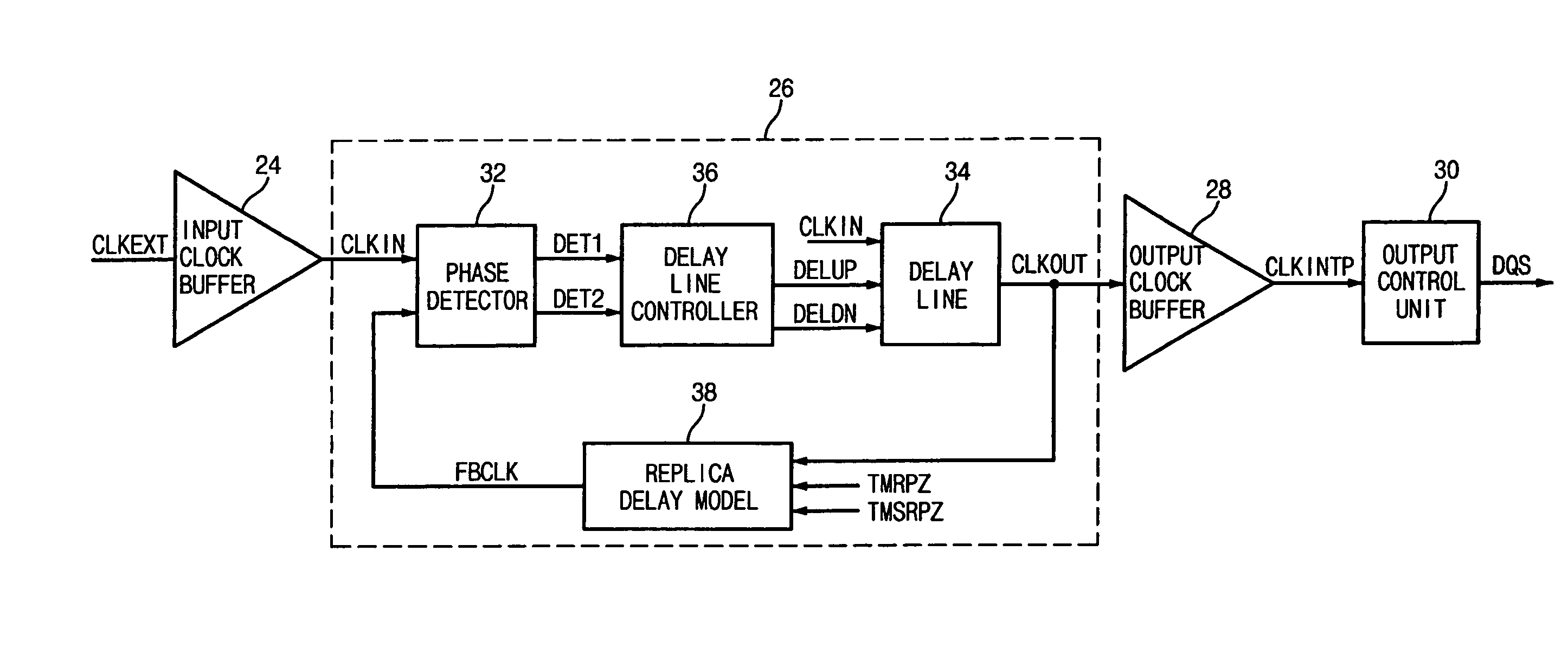
[0057]FIG. 6 is a block diagram illustrating a memory device including a DLL according to an embodiment of the present invention.

[0058]In an embodiment, the memory device includes an input clock buffer 24, a DLL 26, an output clock buffer 28 and an output control unit 30.

[0059]The input clock buffer 24 buffers an externally inputted external clock CLKEXT to an internal clock CLKIN.

[0060]The DLL 26 includes a phase detector 32, a delay line 34, a delay line controller 36 and a replica delay model 38. The phase detector 32 compares a phase of an internal clock CLKIN outputted from the input clock buffer 24 with that of a feedback clock FBCLK fed back through an internal clock. The delay line 34 delays a phase of the internal clock CLKIN. The delay line controller 36 regulates a delay ratio of the delay line 34 in response to a phase detecting signal outputted from the phase detector 32....


PUM


Abstract

A memory device minimizes the skew between an external clock and a DQS (or DQ) after the locking state by regulating a delay ratio of a replica delay model to compensate errors of process, temperature or voltage change. The memory device comprises: an input clock buffer for buffering an externally inputted external clock to generate an internal clock; a DLL for delaying the internal clock to synchronize a phase of the external clock with that of a DQS; an output clock buffer for buffering an output clock outputted from the DLL; and an output control unit for generating the DQS using a clock outputted from the output clock buffer. Here, the DLL comprises a replica delay model for modeling delay factors of the input clock buffer and other delay factors until the output clock outputted from the delay line is outputted to the outside of a chip, and for regulating a delay ratio in response to a plurality of control signals inputted externally in a test mode.

Description

BACKGROUND OF THE INVENTION[0001]1. Field of the Invention[0002]The present invention generally relates to a memory device including a delay locked loop (hereinafter, referred to as “DLL”), and more specifically, to a memory device including a DLL which is configured to minimize the skew an external clock and a DQS (or a DQ) after locking by compensating errors generated from process errors by a delay ratio of a replica delay model and from temperature or voltage change.[0003]2. Description of the Prior Art[0004]In general, a DLL is a circuit for controlling timing of data outputted externally from a DRAM by using an externally inputted external clock of the DRAM. In order to transmit data to a chipset without errors, the DRAM is required to be synchronized with the chipset at the same clock.[0005]That is, when an externally inputted clock is inputted into the inside of the DRAM, a phase is delayed by logic circuits such as an clock input buffer, line loading and a data output buffe...

Claims


Application Information

Patent Timeline
Patent Type & Authority Patents(United States)
IPC IPC(8): G11C8/00H03L7/081G06F1/10G11C7/22G11C11/407G11C11/4076G11C29/02H03K5/13H03L7/06
CPCG11C7/22G11C7/222G11C11/4076H03L7/0814G11C29/023G11C29/028G11C29/50012G11C29/02H03L7/0816F15B15/261F15B2211/7051F15B2211/72
Inventor JANG, EUN JUNGLEE, HYUNG DONG
Owner SK HYNIX INC
Why Eureka
Try Eureka