Optical waveguides and grating structures fabricated using polymeric dielectric compositions

a technology of polymer dielectric composition and optical waveguide, which is applied in the field of optical waveguide and grating production methods, can solve the problems of reducing the cost of fiber optic components, installing, upgrading or expanding a fiber optic network system, and significant impact on the cost-per-customer of delivering additional telecommunication services, and achieves the effect of more dimensional precision

Inactive Publication Date: 2006-01-10
PENN STATE RES FOUND
View PDF9 Cites 12 Cited by
  • Summary
  • Abstract
  • Description
  • Claims
  • Application Information

AI Technical Summary

Problems solved by technology

The cost of installing, upgrading or expanding a fiber optic network system is typically dominated by 2 factors: cost of installation and cost of the fiber optic components.
Lowering the cost of fiber optic components could make a significant impact on cost-per-customer of delivering additional telecommunications services.
One factor involved in the cost of manufacturing fiber optic components employing integrated optical elements is the cost of fabricating the actual chip that contains the optical waveguides, gratings, etc.

Method used


Image

  • Optical waveguides and grating structures fabricated using polymeric dielectric compositions
  • Optical waveguides and grating structures fabricated using polymeric dielectric compositions
  • Optical waveguides and grating structures fabricated using polymeric dielectric compositions

Examples


example 1

BCB Core Waveguide with Integrated BCB Grating

[0059]The following example describes a fabrication process for integrating a grating on the top surface of an optical waveguide where both the grating and core waveguide material are, for example, composed of BCB. The waveguide material can be a different material, formed using an entirely different process. Moreover, the waveguide and / or grating material can be fabricated using other optically suitable materials that can be patterned using electron beam and / or optical lithography.

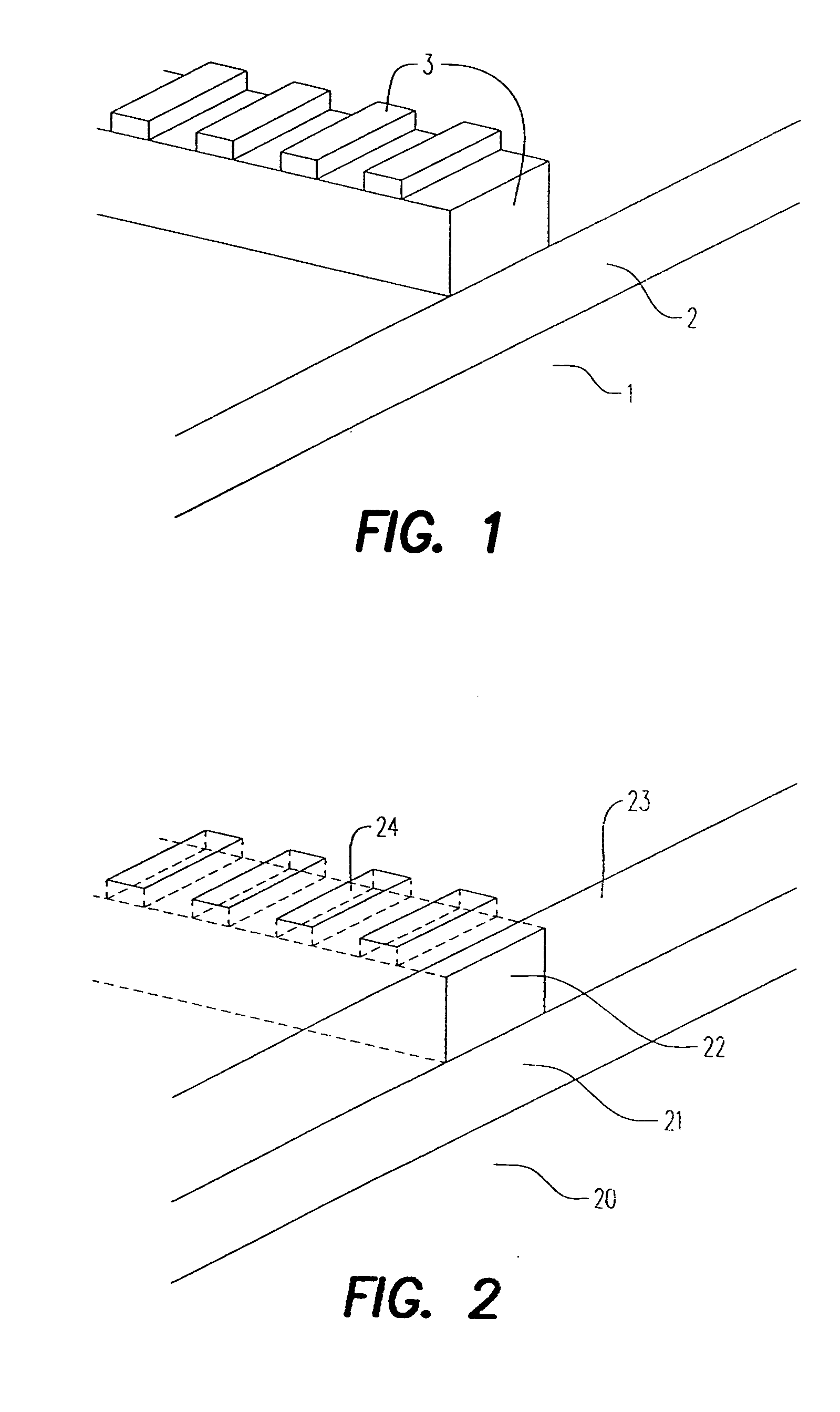
[0060]FIG. 1 depicts a schematic illustration of the final structure. One key element in the process involves a second spin deposition of BCB over a BCB waveguide as outlined below. A key in this process is the planarization properties of BCB. BCB can exhibit approximately 90% planarization or, at times, more, leaving the surface of a substrate with features of 1 micron or 2 microns or 3 microns in depth planar to within less than 0.5 microns or in some cases ...

example 2

BCB Cladding Waveguide with Integrated BCB Grating

[0063]This example is similar to Example 1 except the BCB material is used as a cladding material as well as a grating material. Other suitable optical materials may be used which can be patterned using electron beam or optical lithography. A unique aspect of this process is that the waveguide core material can be any optically suitable material which provides an index of refraction appropriate for the design of the waveguide desired. FIG. 2 is a schematic illustration of the final structure. The general process for fabricating the structure is given below.

An example of a process for fabricating a waveguide with a BCB cladding and integrated grating is summarized below.

[0064]

Example 2 - Waveguide with BCB core and integrated gratingJMC / GPLStep 1Deposit lowerDeposit SiO2 or other suitableeMask means an electroniccladding materialcladding material. This step ismask file used by the e-beamnot needed if the substrate isGlass or other opt...

example 3

BCB Cladding With BCB Grating Fabricated on Surface

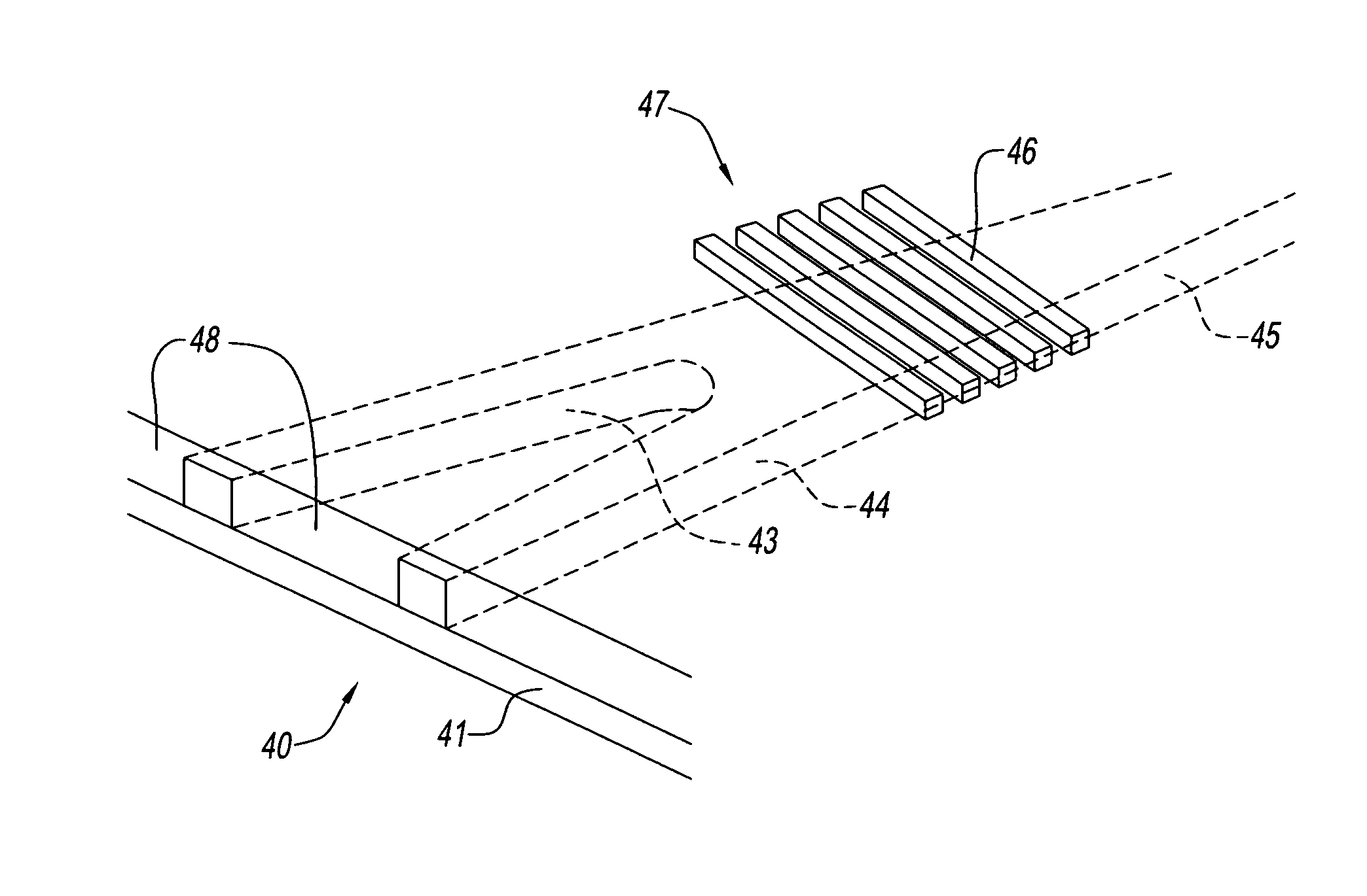
[0065]More complex grating structures can be integrated with a waveguide using BCB as a cladding material by curing the BCB fully (no exposure or development) and either 1) Applying an additional thinner layer of BCB (BCB can be thinned by adding Dow T1100, which is B-staged divinylsiloxane-bis-20–39%, benzocyclobutene Mesitylene 61–70%, Polymerized 1,2-Dihydro-2,2,4-trimethyl quinoline 0.01–10%) on top of the cured BCB (which is insensitive to further optical exposure to electron beam exposure), expose a grating structure using either electron beam or optical lithography and then develop the grating, or 2) Applying an additional layer of another material, such as BCB, curing if required, and then applying another masking material, patterning, developing and etching the grating structure.

[0066]Process 1) above is summarized below and a sample structure is shown schematically in FIG. 3.

An example of a process for fabricating a wavegu...


PUM

PropertyMeasurementUnit
sizeaaaaaaaaaa
wavelengthaaaaaaaaaa
temperatureaaaaaaaaaa

Abstract

Using polymeric dielectric materials (preferably materials derived from bisbenzocyclobutene monomers) and an electron beam lithography process for patterning this material, we have developed a process for fabricating optical waveguides with complex integrated devices such as gratings. Such gratings are not limited to one-dimensional type gratings but can include 2 dimensional gratings such as curved gratings or photonic crystals. Due to the properties of BCB, this process could also be implemented using optical photolithography depending upon the waveguide dimensions desired and the grating dimensions desired. Alternatively, the optical waveguide could be patterned using optical lithography and the grating can be patterned using electron beam lithography. In addition, the general process described below can be applied to the fabrication of complex lightwave circuits containing, for example, multiple optical waveguides, couplers / splitters, grating based filters and even more complex devices and structures.

Description

[0001]This application claims priority from U.S. Provisional Application No. 60 / 307,908 filed Jul. 26, 2001. This application also claims priority from and is a Divisional of U.S. patent application Ser. No. 10 / 206,144, Filed on Jul. 26, 2002 now U.S. Pat. No. 6,826,333.BACKGROUND OF THE INVENTION[0002]1. Field of the Invention[0003]The present invention relates to a novel production method for optical waveguides and gratings and related devices. More particularly, the invention relates to a method of fabricating optical devices including waveguides and gratings using photosensitive polymeric dielectric compositions using electron beam lithography.[0004]2. Description of the Prior Art[0005]Optical devices employing waveguides and / or some type of wavelength selective device such as a grating are of critical importance to the fiber optic telecommunications industry. Optical telecommunications systems employing technologies such as Wavelength Division Multiplexing (WDM) use a variety o...

Claims


Application Information

Patent Timeline
Patent Type & Authority Patents(United States)
IPC IPC(8): G02B6/10G02B6/00G02B6/12G02B6/122G02B6/124G02B6/34G02B6/42G02F1/01G02F1/065
CPCB82Y20/00G02B6/12004G02B6/1221G02B6/1225G02B6/124G02F1/065G02B6/4214G02F2201/30G02B6/4249G02B2006/12097G02F1/0147
Inventor CATCHMARK, JEFFREY M.LAVALLEE, GUY P.
Owner PENN STATE RES FOUND
Why Eureka
Try Eureka