Light emitting diode having an adhesive layer and a reflective layer

a light emitting diode and reflective technology, applied in the field can solve the problems of low light emitting efficiency of led, insufficient bonding effect, and reduced brightness of led, so as to improve mechanical strength, increase the brightness of light emitting diodes, and enhance bonding forces

Inactive Publication Date: 2006-01-17
EPISTAR CORP
View PDF7 Cites 30 Cited by
  • Summary
  • Abstract
  • Description
  • Claims
  • Application Information

AI Technical Summary

Benefits of technology

[0009]An object of the invention is to provide a light emitting diode having an adhesive layer and a reflective layer and the manufacturing method thereof. In the manufacturing method, a transparent adhesive layer is used to bond an LED stack and a substrate having a reflective layer so that light can pass through the transparent adhesive layer and reflected at the reflective layer. On each of the upper and lower surfaces of the transparent adhesive layer is formed a reaction layer. The reaction layer creates reaction when it and the transparent adhesive layer is pressurized and heated to enhance the bonding forces at the adhesive surface for improving mechanical strength. The light directed to the reflective layer is reflected out to increase the brightness of the light emitting diode. Additionally, the reflective layer can also be formed between the LED stack and the reaction layer so that the adhesive layer does not have to be limited to a transparent adhesive layer and light directed to the reflective layer can be reflected out even a non-transparent adhesive layer is used. This method does not have any problems relating the decrease in reflectivity and decrease in bonding effect. Thereby, an effect of total reflection can be obtained and the object of increasing the brightness of an LED can be achieved.

Problems solved by technology

However, it has a disadvantage in that van der Waals forces are too weak to provide a sufficient mechanical bonding strength between the two parts and therefore they are apt to separate.
However, this prior art method has to be carried out at about 1000° C. by exerting a coaxial compressive force on the LED stack and the transparent substrate to form an ohmic interface therebetween.
The primary disadvantage of this prior art method lies in that the property of the LED is destroyed by the high temperature during the manufacturing process and this results in an LED of low light emitting efficiency.
It therefore reduces brightness of the LED.
One of the disadvantages lies in that although a low bonding temperature will not cause any reaction between the metal layer and any of the two semiconductor layers to be bonded and therefore a highly reflective metal surface (reflectivity over 90%) and improved light emitting efficiency can be obtained, the bonding effect is not sufficient due to that there is no reaction between the metal layer and any of the semiconductor layers to be bonded, and an ohmic interface cannot be formed between the metal layer and any of the semiconductor layers to be bonded.
However, the reflectivity of the reflective metal layer will be greatly reduced and therefore the metal layer cannot provide a good mirror function.
This is another disadvantage of the bonding technique.
However, if the metal layer is simply adhered to the LED stack by use of an adhesive layer, the adhesion between them is achieved only by van der Waals forces and peeling is apt to occur at the adhesion interface.

Method used


Image

  • Light emitting diode having an adhesive layer and a reflective layer
  • Light emitting diode having an adhesive layer and a reflective layer
  • Light emitting diode having an adhesive layer and a reflective layer

Examples


Embodiment Construction

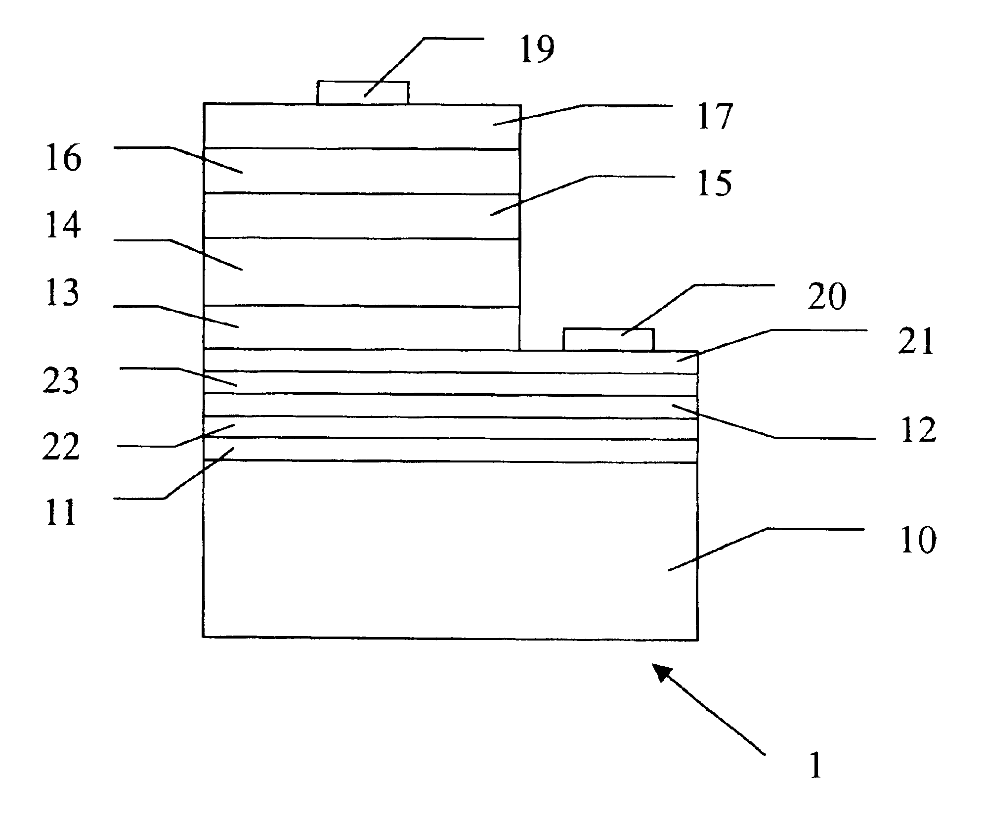
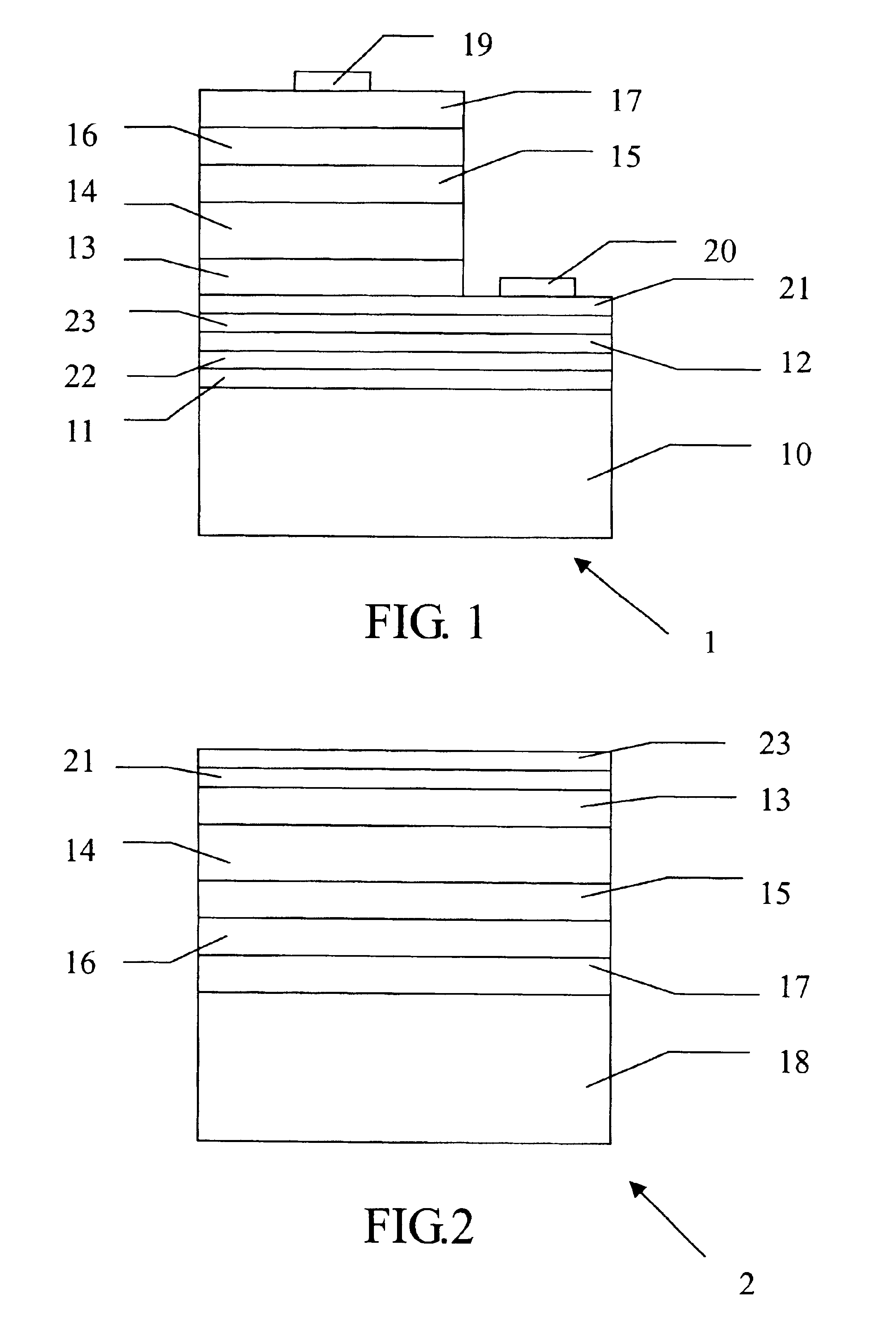
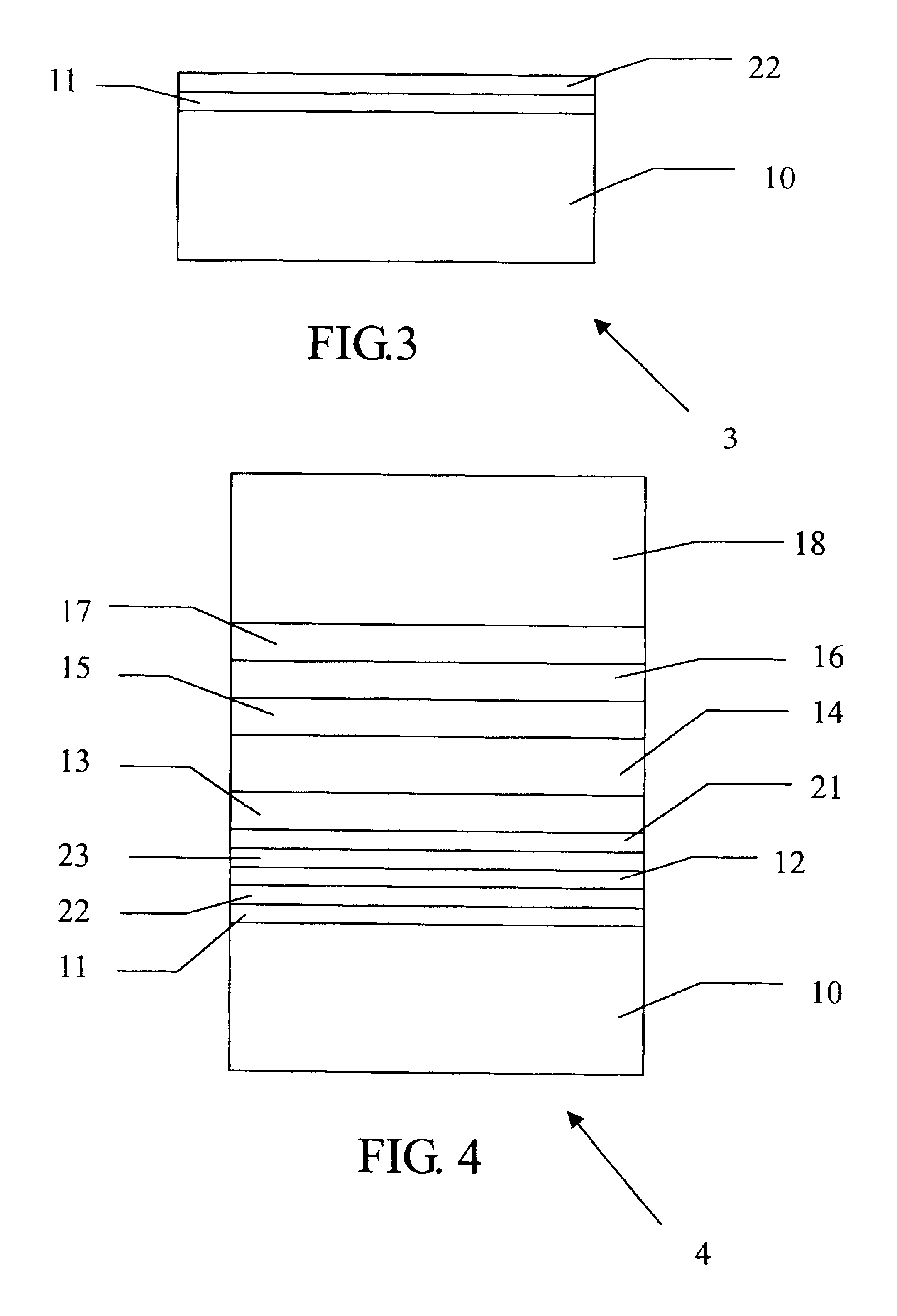
[0026]Referring to FIG. 1, a light emitting diode having an adhesive layer and a reflective layer 1 in accordance with a preferred embodiment of the invention comprises a second substrate 10, a reflective metal layer 11 formed on the second substrate 10, a first reaction layer 22 formed on the reflective metal layer 11, a transparent adhesive layer 12 formed on the first reaction layer 22, a second reaction layer 23 formed on the transparent adhesive layer 12, a transparent conductive layer 21 formed on the second reaction layer 23, wherein the upper surface of the transparent conductive layer 21 consists of a first surface area and a second surface area. A first contact layer 13 is formed on the first surface area. A first cladding layer 14 is formed on the first contact layer 13. An active layer 15 is formed on the first cladding layer 14. A second cladding layer 16 is formed on the active layer 15. A second contact layer 17 is formed on the second cladding layer 16. A first elect...


PUM


Abstract

A light emitting diode having an adhesive layer and a reflective layer and a manufacturing method thereof featured by adhering together a light emitting diode stack and a substrate having a reflective metal layer by use of a transparent adhesive layer so that the light rays directed to the reflective metal layer can be reflected therefrom to improve the brightness of the light emitting diode.

Description

BACKGROUND OF INVENTION[0001]1. Field of the Invention[0002]The present invention relates to a light emitting diode and the manufacturing method thereof. More particularly, the invention is directed to a light emitting diode having an adhesive layer and a reflective layer and the manufacturing method thereof.[0003]2. Description of the Prior Art[0004]Light emitting diodes can be used in a wide variety of devices, for example, optical displays, traffic lights, data storage devices, communication devices, illumination devices, and medical devices. To manufacture a light emitting diode of higher brightness is an important task of engineers.[0005]A prior art method for improving LED brightness involves bonding two semiconductor parts together by van der Waals forces. However, it has a disadvantage in that van der Waals forces are too weak to provide a sufficient mechanical bonding strength between the two parts and therefore they are apt to separate.[0006]In U.S. Pat. No. 5,376,580, a m...

Claims


Application Information

Patent Timeline
Patent Type & Authority Patents(United States)
IPC IPC(8): H01L33/00H01L27/15H01L31/12H01L33/10H01L29/08H01L33/30H01L33/34H01L33/42H01L33/46
CPCH01L33/0079H01L33/46H01L33/405H01L33/42H01L33/0093
Inventor LIU, WEN-HUANGTSENG, TZU-FENGHSIEH, MIN-HSUNYEH, TING-WEIWANG, JEN-SHUI
Owner EPISTAR CORP
Why Eureka
Try Eureka