Substrate for electrooptic device and method of manufacturing the same, electrooptic device, and electronic equipment

a technology of electrooptic devices and substrates, applied in the direction of optics, identification means, instruments, etc., can solve the problems of inability to achieve sufficient brightness, and low so as to shorten the manufacturing process, reduce the brightness of an image display, and increase the utilization efficiency of transmitted light

Inactive Publication Date: 2006-01-17
BOE TECH GRP CO LTD
View PDF14 Cites 8 Cited by
  • Summary
  • Abstract
  • Description
  • Claims
  • Application Information

AI Technical Summary

Benefits of technology

[0020]When a case is considered where the substrate for an electrooptic device as has the above construction is applied to the electrooptic device, for example, a liquid crystal device, the utilization efficiency of transmitted light in a transmission type display can be heightened without lowering the brightness of an image display in a reflection type display. Further, when the brightness of the transmitted light is sufficiently ensured by heightening the utilization efficiency of the transmitted light, the area of the transmission portion may be reduced, that is, to increase the area of the reflection portion, whereby the reflection type display usually liable to darken can be brightened.
[0025]When a case is considered where the substrate for an electrooptic device having the above construction is applied to the electrooptic device, for example, a liquid crystal device, the utilization efficiency of transmitted light in a transmission type display can be heightened without lowering the brightness of an image display in a reflection type display. Further, due to the existence of the underlayer, the passing distance of reflected light can be shortened, whereby reflection characteristics in the reflection display can be enhanced.
[0030]When a case is considered where the substrate for an electrooptic device having the above construction is applied to the electrooptic device, for example, a liquid crystal device, the orientation film makes the orientation of the liquid crystal layer uniform so as to effectively polarize light, whereby the utilization efficiency of the transmitted light in a transmission type display can be heightened without lowering the brightness of an image display in a reflection type display.
[0032]When a case is considered where the manufacturing method of this construction is applied to the electrooptic device, for example, a liquid crystal device, it is possible to manufacture a substrate for an electrooptic device which heightens the utilization efficiency of transmitted light in a transmission type display without lowering the brightness of an image display in a reflection type display. Furthermore, since the insulating layer can be utilized as the mask in the case of exposing the reflection layer to light, a manufacturing process can be shortened, and hence, the substrate for the electrooptic device can be manufactured easily and at low cost.

Problems solved by technology

The liquid crystal device 1000 of such a semitransmissive reflection type, however, has had problems as stated below, due to the adoption of the two different display schemes of the reflection type display and the transmission type display.
Thus, when the thickness of the liquid crystal layer is determined so that the retardation value (Δn·d) may become the optimum value in the reflection type display usually liable to darken, there has been the problem that, in the transmission type display, the utilization efficiency of the transmitted light becomes low, so a sufficient brightness cannot be attained.
However, there has been the problem that, when the area of each transmission portion 1011a is decreased, the brightness of the transmission type display lowers.
As stated above, brightening the reflection type display and brightening the transmission type display are in an antinomic relationship (i.e., contradictory), and there has been the problem that the compatibility of the two is very difficult.
This has resulted in the problem that various characteristics required of electronic equipment, especially portable type equipment, such as reducing the size of the liquid crystal device, thinning the structure thereof, reducing the weight thereof and lowering the power consumption thereof, cannot be satisfactorily met.

Method used


Image

  • Substrate for electrooptic device and method of manufacturing the same, electrooptic device, and electronic equipment
  • Substrate for electrooptic device and method of manufacturing the same, electrooptic device, and electronic equipment
  • Substrate for electrooptic device and method of manufacturing the same, electrooptic device, and electronic equipment

Examples


first embodiment

[0060

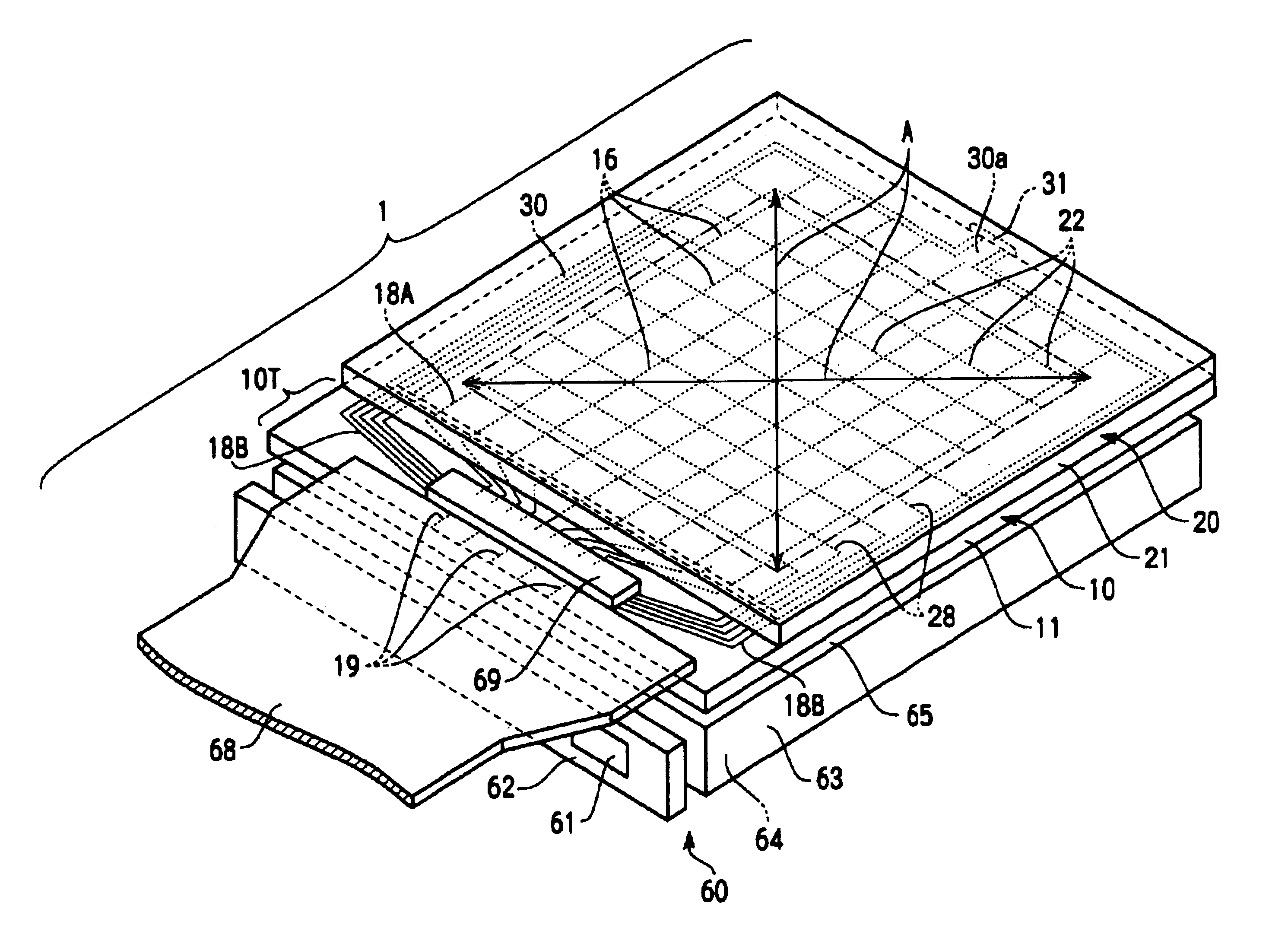
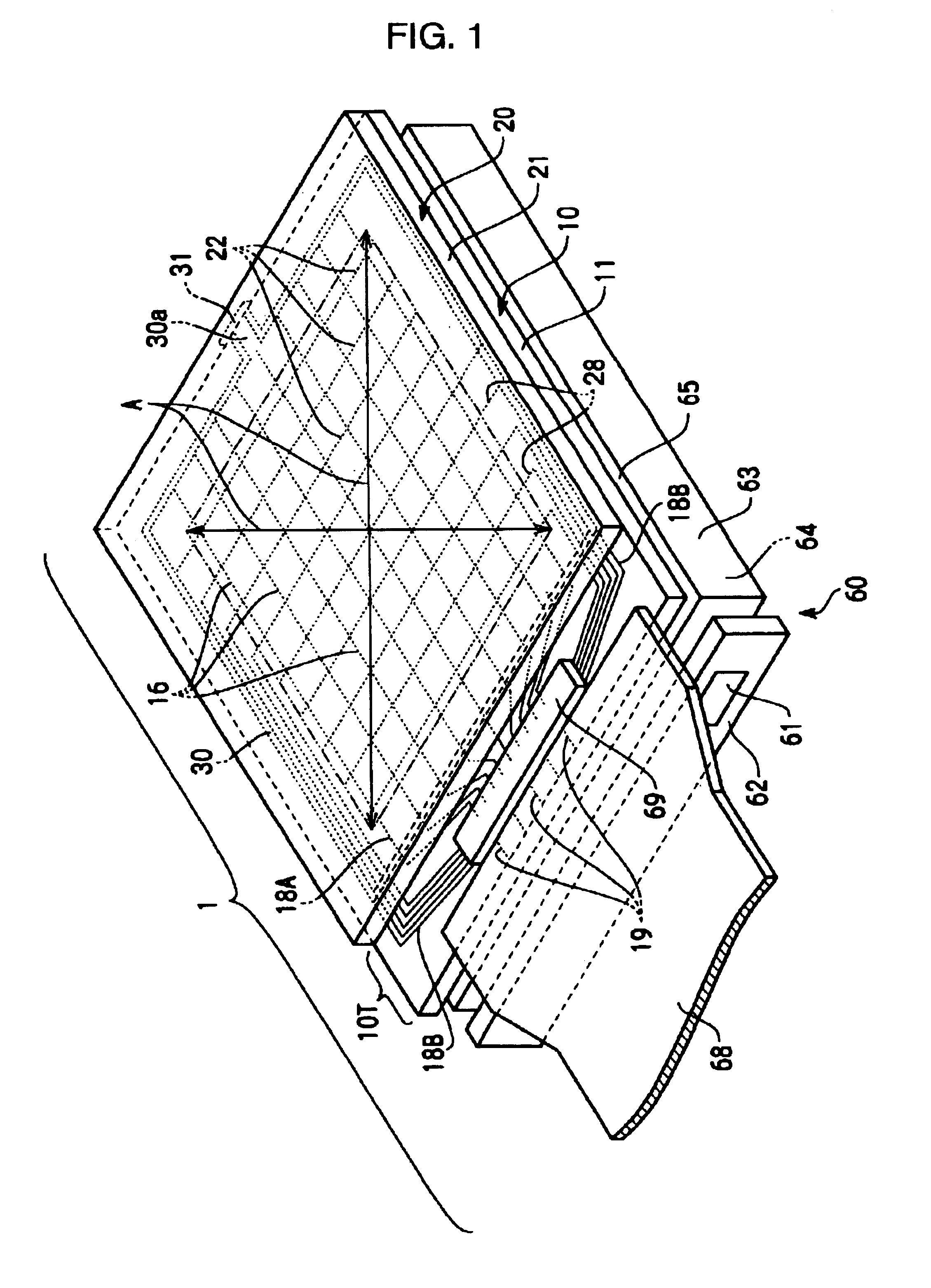
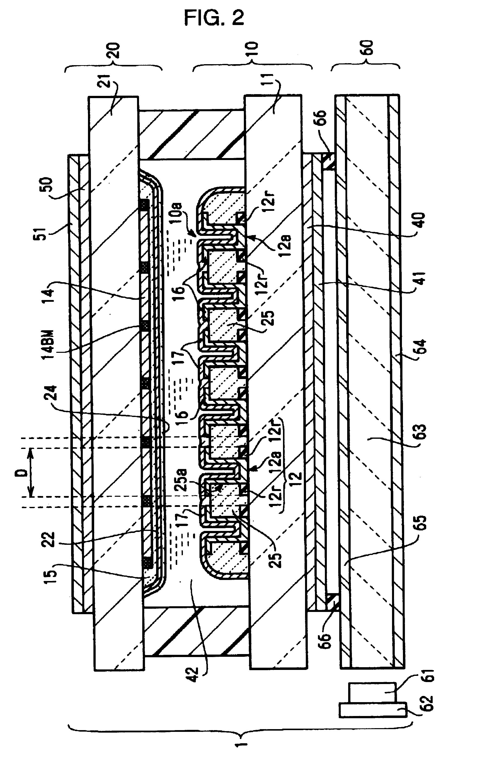
[0061]First, a liquid crystal device which is one embodiment of the electrooptic device of the present invention will be described with reference to FIGS. 1 through 4. FIG. 1 shows the external appearance structure of the liquid crystal device in this embodiment. FIG. 2 shows the sectional structure of the liquid crystal device. FIG. 3 shows several display dot parts in a substrate for the liquid crystal device as constitutes this liquid crystal device, in plane and on an enlarged scale. FIG. 4 shows portions in FIG. 2 on an enlarged scale. Incidentally, a liquid crystal device 1 shown here is one of passive matrix scheme of so-called “semitransmissive reflection type”.

[0062]As shown in FIG. 1, the liquid crystal device 1 includes a substrate for the liquid crystal device 10, whose basic body is a first base member 11 made of a glass plate, a synthetic resin plate or the like and being transparent or having light transmissivity, and an opposing substrate 20 whose basic body is ...

second embodiment

[0102

[0103]Next, a liquid crystal device which is another embodiment of the electrooptic device according to the present invention will be described with reference to FIGS. 6 through 8. FIG. 6 shows the sectional structure of the principal portions of the liquid crystal device 101. FIG. 7 is a plan view in which a substrate for the liquid crystal device as constitutes the liquid crystal device 101 is seen in the plus direction of a Z-axis in FIG. 6. FIG. 8 is a plan view in which an opposing substrate constituting the liquid crystal device 101 is seen in the plus direction of the Z-axis in FIG. 6. Incidentally, FIG. 6 is a sectional view taken along line X1-X1′ in FIG. 7 and line X2-X2′ in FIG. 8.

[0104]The liquid crystal device 101 is a liquid crystal device of active matrix scheme employing TFD (Thin Film Diode) elements as active elements. Referring to FIG. 6, the opposing substrate 120 is provided with each transparent electrode 122 which is arranged so as to coincide with a corr...

third embodiment

[0117

[0118]Next, a liquid crystal device which is another embodiment of the electrooptic device according to the present invention will be described with reference to FIGS. 9 and 10. FIG. 9 shows the sectional structure of the principal portions of the liquid crystal device 201. FIG. 10 shows a plane structure in the case where an opposing substrate 220 constituting the liquid crystal device 201 is seen in the minus direction of a Z-axis in FIG. 9. The opposing substrate 220 is sometimes called the “color filter array substrate”. Incidentally, FIG. 9 is a sectional view taken along line X3-X3′ in FIG. 10. This embodiment is the liquid crystal device of active matrix scheme in which TFT (Thin Film Transistor) elements 230 being active elements of 3-terminal type are employed as the active elements.

[0119]Referring to FIG. 9, the opposing substrate 220 is the color filter array substrate provided with each transparent electrode 222 which is arranged so as to coincide with a correspondi...


PUM

PropertyMeasurementUnit
transmission factoraaaaaaaaaa
refractive indexaaaaaaaaaa
thicknessaaaaaaaaaa

Abstract

A substrate for an electrooptic device comprising a light-transmissive base member, a reflection layer formed on the base member so as to include each reflection portion and a corresponding transmission portion having a transmission factor higher than that of the reflection portion, a light transmission layer formed over the base member so as to coincide with the reflection layer and to include each hollow at a position that coincides with the transmission portion in plane, and an orientation film formed over the base member so as to coincide with the light transmission layer and to define a concavity while entering the corresponding hollow. The thickness “b” of a liquid crystal layer corresponding to the concavity is greater than the thickness “a” of the liquid crystal layer at the other positions thereof.

Description

DETAILED DESCRIPTION OF THE INVENTION[0001]1. Technical Field to which the Invention Belongs[0002]The present invention relates to a substrate for use in an electrooptic device such as a liquid crystal device or an organic EL device, as well as a method of manufacturing the substrate, the electrooptic device such as the liquid crystal device, and an electronic equipment constructed by employing the electrooptic device.[0003]2. Prior Art[0004]There has heretofore been known an electrooptic device, for example, a liquid crystal device of a semitransmissive reflection type wherein both reflection type display utilizing external light and transmission type display utilizing light from an illuminator such as backlighting unit can be visually recognized. With the liquid crystal device of the semitransmissive reflection type, a reflection layer for reflecting the external light is disposed at an inner part, and the illuminating light from the backlighting unit or the like can be transmitte...

Claims


Application Information

Patent Timeline
Patent Type & Authority Patents(United States)
IPC IPC(8): G02F1/00G02F1/1333G02F1/1335G02F1/1337G02F1/1343G09F9/30G09F9/35
CPCG02F1/133555G02F1/133371G02F1/133345G09G2300/0456G02F1/1335
Inventor OTAGIRI, YOSHIHIROTAKIZAWA, KEIJINAKANO, TOMOYUKIKANEKO, HIDEKITANAKA, CHIHIRO
Owner BOE TECH GRP CO LTD
Why Eureka
Try Eureka