Method for application of gating signal in insulated double gate FET

Inactive Publication Date: 2006-01-24
NAT INST OF ADVANCED IND SCI & TECH
View PDF7 Cites 58 Cited by
  • Summary
  • Abstract
  • Description
  • Claims
  • Application Information

AI Technical Summary

Benefits of technology

[0016]FIG. 2(b) depicting a waveform having both rise and fall delayed or advanced, FIG. 2(c) depicting a waveform delayed or advanced, and FIG. 2(d) depicts a waveform of a constant potential in accordance w

Problems solved by technology

This point brings up the problem of decline in yield to an integrated circuit that uses an extremely large number of elements.
The metal, however, allows no fine control of the work function because the work function has a discrete value for metal to metal.
This method, however, is at a disadvantage in complicating the process to be used for the production.
Since the electric current flows only through the channel on the signal input gate side, this method is at a disadvantage in suffering the amount of electric curren

Method used


Image

  • Method for application of gating signal in insulated double gate FET
  • Method for application of gating signal in insulated double gate FET
  • Method for application of gating signal in insulated double gate FET

Examples


Embodiment Construction

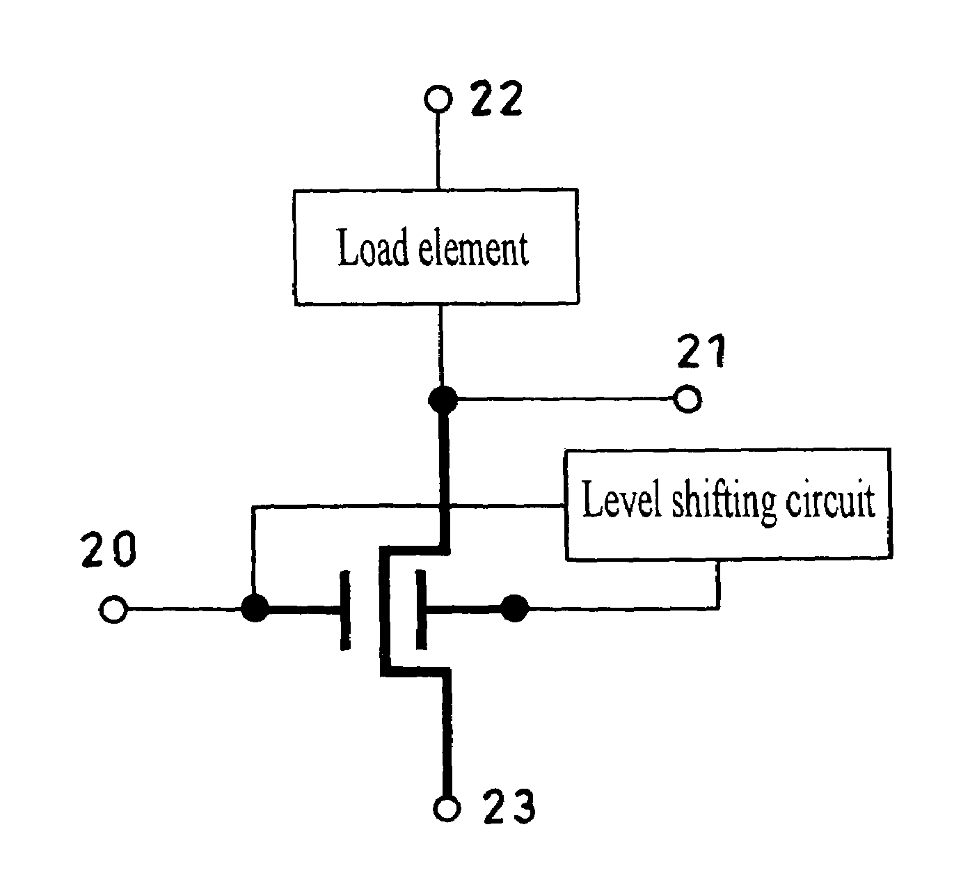
[0027]The method for the application of a gating signal in an insulated double gate FET according to this invention comprises applying an input signal for ordinary logical operation to one of the gate electrodes of the insulated double gate FET during the operation of transient response and applying to the other gate electrode a signal having a temporal change of a signal level in one and the same direction as the signal first mentioned above (hereinafter referred to “in-phase”), which (i) has at least one of the low level and the high level of the signal shifted by a predetermined magnitude or (ii) has the slower or faster signal level change or (iii) has admitted a predetermined time difference (advance or delay).

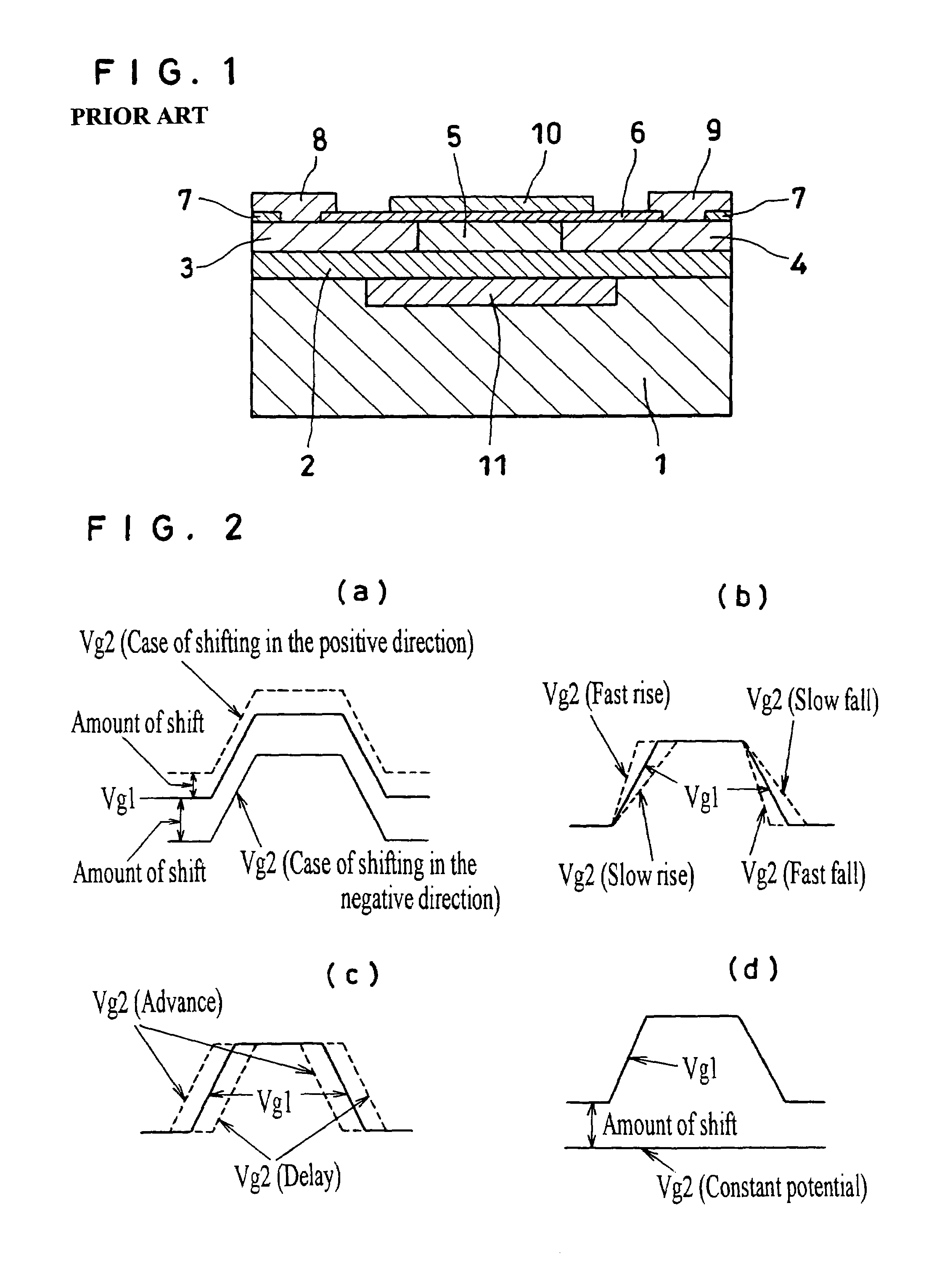
[0028]FIG. 2 schematically explains the temporal relation between the waveform of an input signal Vg1 to a gate electrode 1 and the waveform of an input signal Vg2 to a gate electrode 2. FIG. 2(a) illustrates the first method of this invention that uses the input signal V...


PUM


Abstract

In an insulated double gate FET, the threshold voltage during the operation of a transient response thereof is enabled to be arbitrarily and accurately controlled by a method that includes applying a first input signal intended to perform an ordinary logic operation to one of the gate electrodes thereof and applying, in response to this signal, a second signal that has a signal-level temporal-change direction as the first input signal and has at least one of the low level and the high level thereof shifted by a predetermined magnitude or endowed with a predetermined time difference or has the time slower or faster signal level change of the signal to the other gate electrode.

Description

BACKGROUND OF THE INVENTION[0001]1. Field of the Invention[0002]This invention relates to a method for the application of a gating signal in an insulated double gate field effect transistor (FET).[0003]2. Description of the Prior Art[0004]For the purpose of materializing an insulated gate FET having a minute channel length, the prevention of the so-called short channel effect (sudden fall of threshold voltage occurring when the channel length is shortened) is an indispensable condition.[0005]As one of the element configurations directed toward this prevention, an insulated double gate FET illustrated in FIG. 1 may be adduced, for example (Japanese Patent No. 2021931). In the diagram, 1 denotes a substrate, 2 a second gate insulating film concurrently serving as an insulating layer for separating a semiconductor crystal layer formed on the substrate from the substrate, though not wholly illustrated, 3, 4 and 5 respectively a source region, a drain region and a channel region formed i...

Claims


Application Information

Patent Timeline
IPC IPC(8): H03K17/687H01L21/822G06G7/18H01L27/04H01L29/786H03K3/356H03K17/30
CPCH03K3/356017H03K17/302H03K3/356069H03K2217/0018
Inventor SEKIGAWA, TOSHIHIROKOIKE, HANPEINAKAGAWA, TADASHI
Owner NAT INST OF ADVANCED IND SCI & TECH
Why Eureka
Try Eureka