Circuit board sub-assemblies, methods for manufacturing same, electronic signal filters including same, and methods, for manufacturing electronic signal filters including same

a technology of circuit board and sub-assembly, which is applied in the direction of electrical apparatus construction details, electrical apparatus casings/cabinets/drawers, cross-talk/noise/interference reduction, etc., can solve the problems of high degree of precision, complex and time-consuming required multi-directional axis assembly steps, and unfavorable efficient and effective plating, etc., to achieve the effect of improving production efficiency and reducing costs

Inactive Publication Date: 2006-01-24
EAGLE COMTRONICS
View PDF9 Cites 18 Cited by
  • Summary
  • Abstract
  • Description
  • Claims
  • Application Information

AI Technical Summary

Benefits of technology

[0032]It is an object of the present invention to overcome the drawbacks associated with the prior art ground straps mentioned above. That is, it is an object of the present invention to provide a ground strap that can be assembled to a circuit board while requiring only a minimal amount of circuit board surface, that provides a circuit board sub-assembly having improved strength, and which facilitates an overall manufacturing efficiency improvement.
[0044]The various embodiments of the present invention overcome the drawbacks associated with the prior art ground straps and circuit board sub-assemblies described above in a variety of ways. First, the shoulder portions and the foot pads of the ground strap according to the present invention essentially sandwich the circuit board of the present invention, and the leg portions of the ground strap of the present invention exert outward pressure on a portion of the surface of the through-holes to provide improved Y and Z-axis stability and improved anti-rocking features. Preventing the ground straps of the circuit board sub-assemblies from rocking on the circuit boards as the array is wave soldered is important, for example, because it is desirable for the axis of the ground strap to remain perpendicular to the circuit board during wave soldering, and subsequently, when the circuit board sub-assembly is inserted into a filter housing.
[0045]That is, any deviation from the desired positional relationship between the ground strap and the circuit board of a circuit board sub-assembly is likely to result in misalignment during insertion into a filter housing. Such misfits can disrupt or interfere with providing the proper clearance between the first portion of the ground strap and the inner surface of the filter housing for subsequent soldering that is sufficient to provide the intended electrical communication between the circuit board, the ground strap and the filter housing. Also, the structural integrity of the ground strap can be distorted or damaged if a misaligned sub-assembly is inserted into a filter housing, and the potential for damaging the circuit board during improper assembly is also a concern. These problems are significantly reduced, however, by virtue of the anti-rocking stability provided by the ground strap according to the present invention.
[0047]Moreover, since the ground strap according to the present invention can be assembled onto a circuit board that is provided with a pair of circular through-holes, the circuit board array manufacturing efficiency and the circuit board sub-assembly manufacturing efficiency are improved. For example, the round through-holes formed in the circuit board are easily plated by conventional methods, if plating is desired. Furthermore, the round through-holes are more stress-proof than elongate openings and resist deformation when the singulation channels are formed in the circuit board material to define the individual circuit boards of the array. As such, the round through-holes are not subject to the undesirable deformation that is typically experienced when using slotted circuit boards, and the additional slot formation steps or subsequent slot routing steps associated with the prior slotted circuit boards are not required to prevent or correct these problems.
[0049]Moreover, in the various embodiments of the present invention which include mechanical engagement means for providing solderless grounding contact, the required electrical contact between the filter housing member, the ground strap and the circuit board is provided and the circuit board is grounded without the need for an additional, manual soldering step. This, in turn, improves production efficiency and reduces costs, as well.

Problems solved by technology

There are some electronic signal filter applications, however, that do not require magnetic isolation shielding, and thus, do not include isolation shields that can also be used to provide the required ground connection.
That is, the punch formed surfaces of the notches 110 are not smooth, as compared to drilled or routed surfaces, and that roughened surface structure, in combination with the position on the peripheral edges of the lateral sides of the circuit boards 100, are not conducive to efficient and effective plating.
That is, the required multi-directional-axis assembly steps are more complicated and time consuming than single- axis assembly steps.
Additionally, the close proximity of adjacent ground straps further complicates the process in that a high degree of precision is required to ensure proper assembly of each ground strap and to avoid causing damage to adjacent ground straps during the assembly process.
In that manner, the costs, with respect to both time and parts, are increased.
This additional routing operation is yet another slot formation step that further increases production time and costs, and one that must be specifically directed to those slots 210 that actually experience deformation.

Method used


Image

  • Circuit board sub-assemblies, methods for manufacturing same, electronic signal filters including same, and methods, for manufacturing electronic signal filters including same
  • Circuit board sub-assemblies, methods for manufacturing same, electronic signal filters including same, and methods, for manufacturing electronic signal filters including same
  • Circuit board sub-assemblies, methods for manufacturing same, electronic signal filters including same, and methods, for manufacturing electronic signal filters including same

Examples


Embodiment Construction

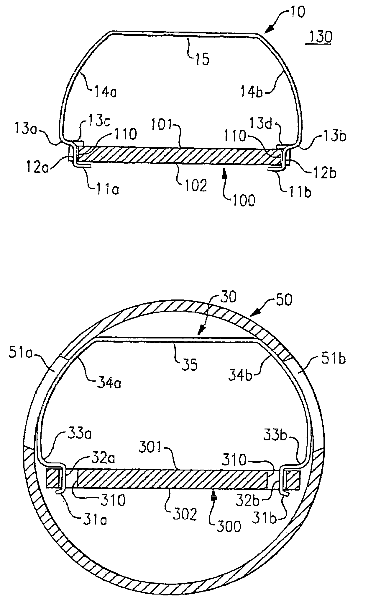
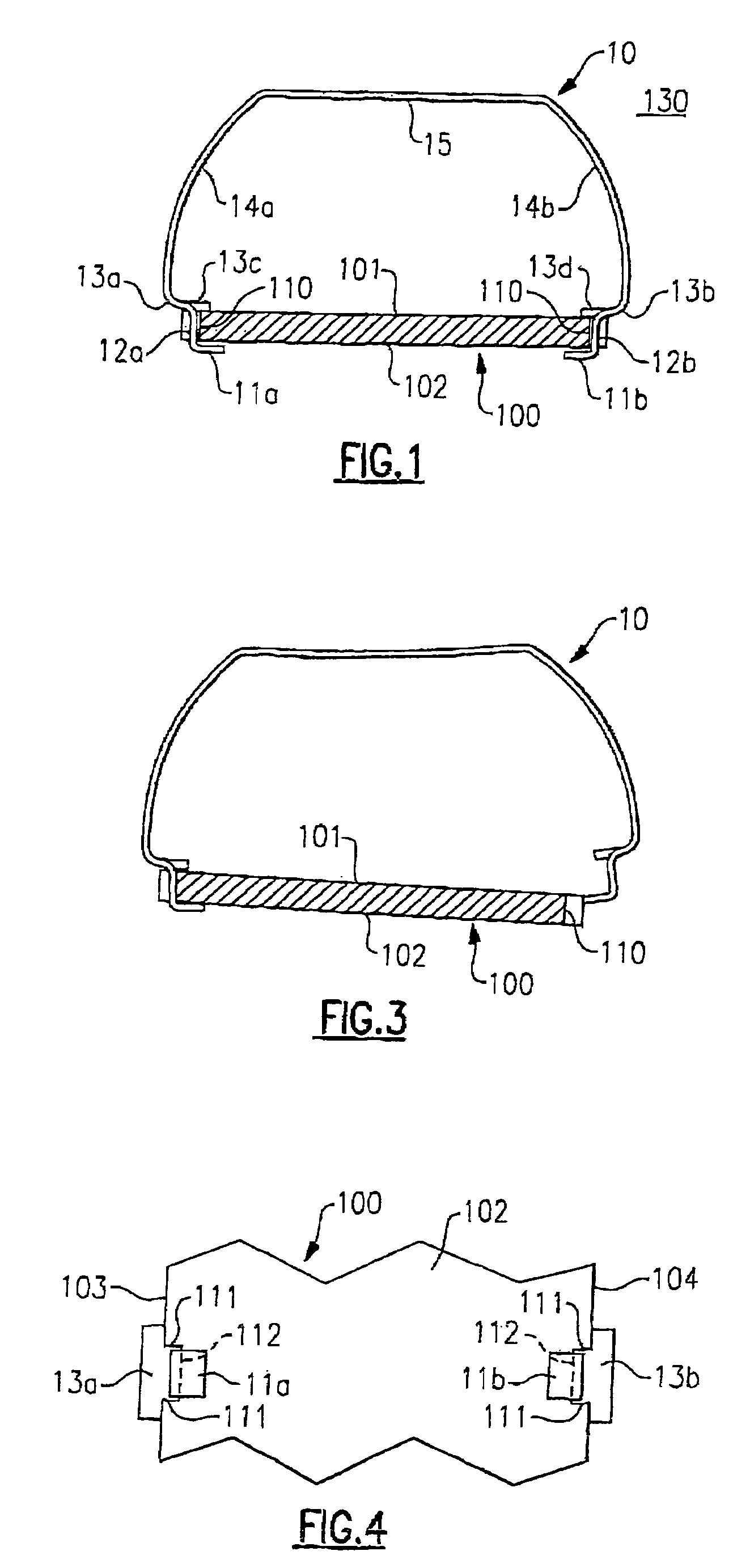
[0070]In an effort to overcome the drawbacks associated with the ground strap 10 and notched circuit board 100 of FIGS. 1–5 and the ground strap 20 and slotted circuit board 200 of FIGS. 6–12, the ground strap 30 according to the present invention, which is shown, for example, in FIG. 13, was developed. According to one embodiment of the present invention, a circuit board sub-assembly 330 is provided, including a circuit board 300 and a ground strap 30 assembled thereon.

[0071]At first glance, it may appear to the untrained eye that when the ground strap 30 is assembled onto the circuit board 300 to form the sub-assembly 330 of FIG. 13, the circuit board sub-assembly 330 looks similar to the circuit board sub-assembly 230 shown in FIG. 6. It should be noted, however, that several important design and efficiency advances are achieved according to the present invention by implementing what might otherwise appear to be incremental changes.

[0072]That is, seemingly incremental design and ...


PUM

PropertyMeasurementUnit
distanceaaaaaaaaaa
distanceaaaaaaaaaa
diameteraaaaaaaaaa

Abstract

An electronic signal filter includes a cylindrical housing and a circuit board positioned therein having a plurality of peripheral edges and at least two circular through-holes formed therein. Each through-hole is inwardly spaced from one of the peripheral edges of the circuit board, defining a first distance between a respective one of the through-holes and a respective peripheral edge of the circuit board and defining a second distance between the through-holes. The filter also includes a ground strap attached to and spaced a distance above the circuit board. The ground strap includes a first portion, an integral second portion residing in and extending through each through-hole, and an integral third portion that contacts a portion of the second surface of the circuit board. At least a portion of the first portion of the ground strap contacts the inner peripheral surface of the cylindrical housing to ground the circuit board.

Description

FIELD OF THE INVENTION[0001]The present invention relates to a circuit board sub-assembly including a ground strap for grounding an electronic component. In particular, the present invention relates to a circuit-board sub-assembly including a ground strap that provides a ground connection between the circuit board and filter housing of an electronic signal filter.BACKGROUND OF THE INVENTION[0002]For electronic signal filter applications that require magnetic isolation shielding between different filter sections, isolation shields are typically soldered to the circuit board. After the circuit board sub-assembly is inserted into an electronic signal filter housing (which is typically grounded), the isolation shields are soldered to the housing to provide a ground connection between the circuit board and the filter housing. There are some electronic signal filter applications, however, that do not require magnetic isolation shielding, and thus, do not include isolation shields that can...

Claims


Application Information

Patent Timeline
Patent Type & Authority Patents(United States)
IPC IPC(8): H05K9/00H05K7/02H05K7/04H05K1/02H05K3/30H05K7/14
CPCH05K1/0215H05K9/0039H05K3/308Y10T29/49126H05K2201/10386
Inventor MAGUIRE, JOSEPH N.ZENNAMO, JR., JOSEPH A.
Owner EAGLE COMTRONICS
Why Eureka
Try Eureka