Process for cleaning silicon surface and fabrication of thin film transistor by the process

Active Publication Date: 2006-01-31
AU OPTRONICS CORP
View PDF22 Cites 8 Cited by
  • Summary
  • Abstract
  • Description
  • Claims
  • Application Information

AI Technical Summary

Benefits of technology

[0009]An object of the present invention is to solve the above-mentioned problems and provide a process for cleaning a silicon surface. The present cleaning process is suitable for all silico

Problems solved by technology

These cleaning methods produce good cleaning results, but suffer from requiring a large amount of chemicals, resulting in environmental problems and additional treatment costs.
CJ and brush cleaning are ineffective on particles smal

Method used


Image

  • Process for cleaning silicon surface and fabrication of thin film transistor by the process
  • Process for cleaning silicon surface and fabrication of thin film transistor by the process
  • Process for cleaning silicon surface and fabrication of thin film transistor by the process

Examples


Example

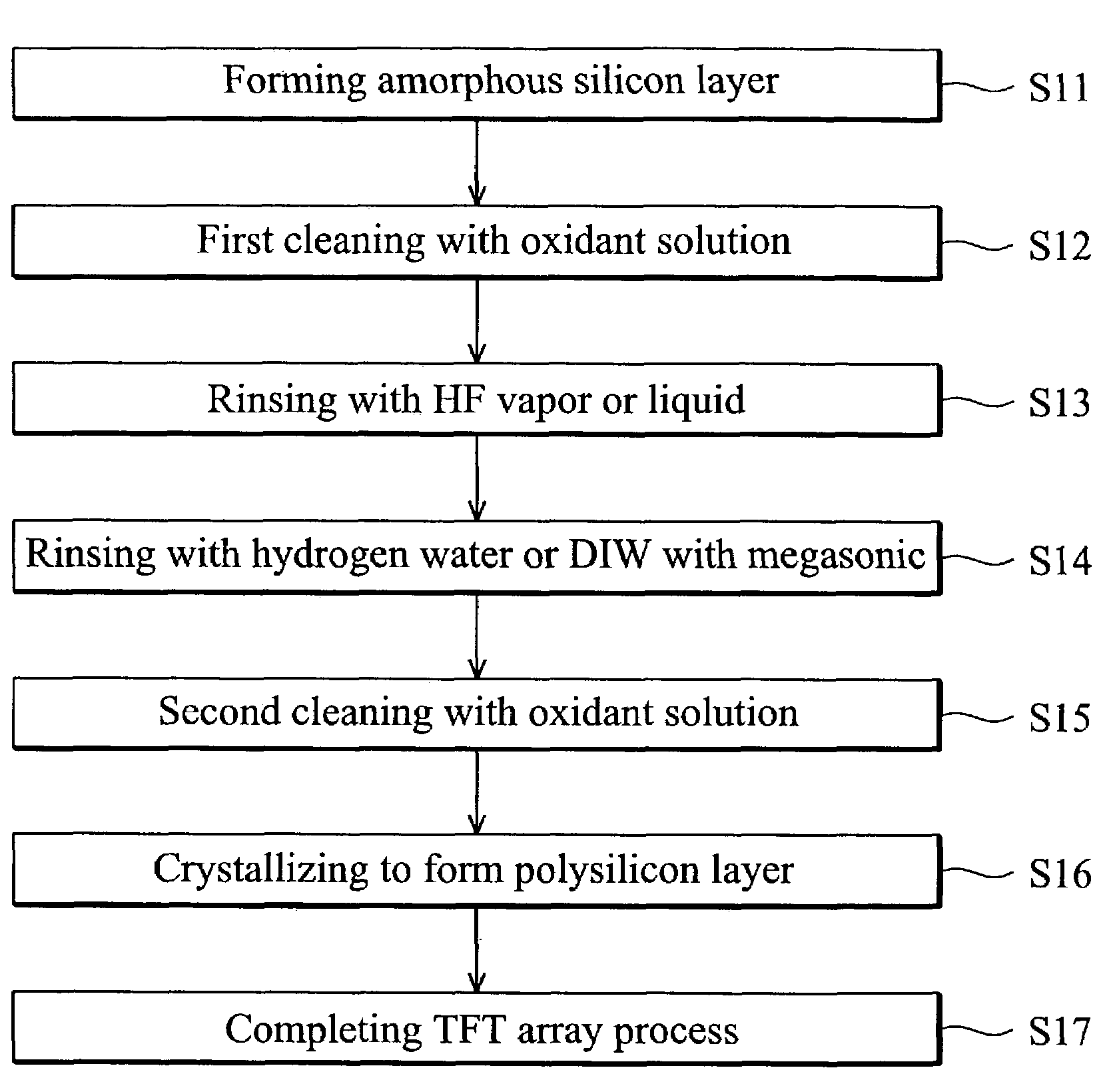
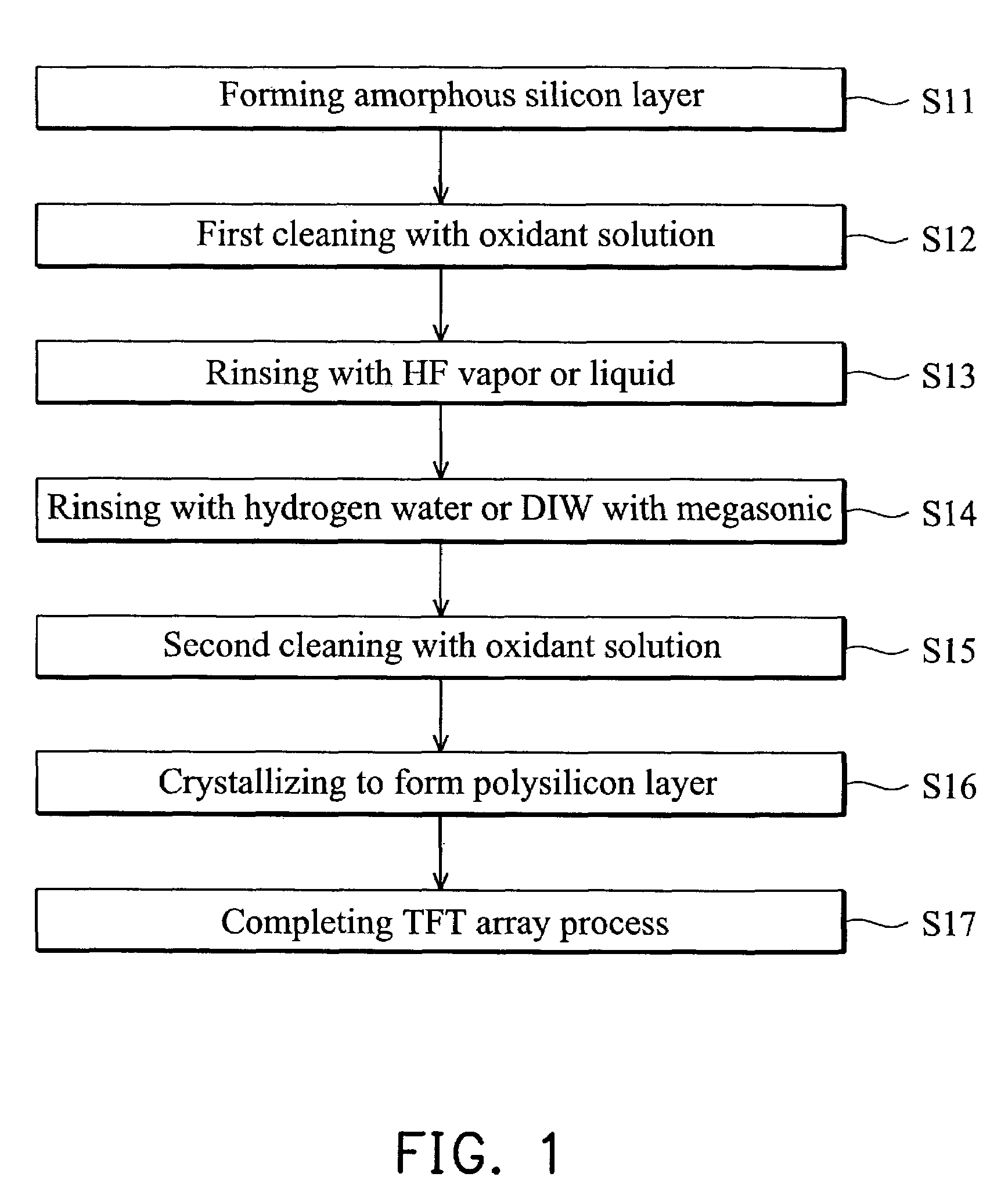
[0017]The present invention provides a cleaning process for silicon surface. First, a silicon surface is cleaned with an oxidant solution for a first time. Then, the silicon surface is rinsed with HF vapor or liquid. Then, the silicon surface is rinsed with hydrogen water or deionized water under megasonic agitation. Finally, the silicon surface is cleaned with an oxidant solution for the second time.

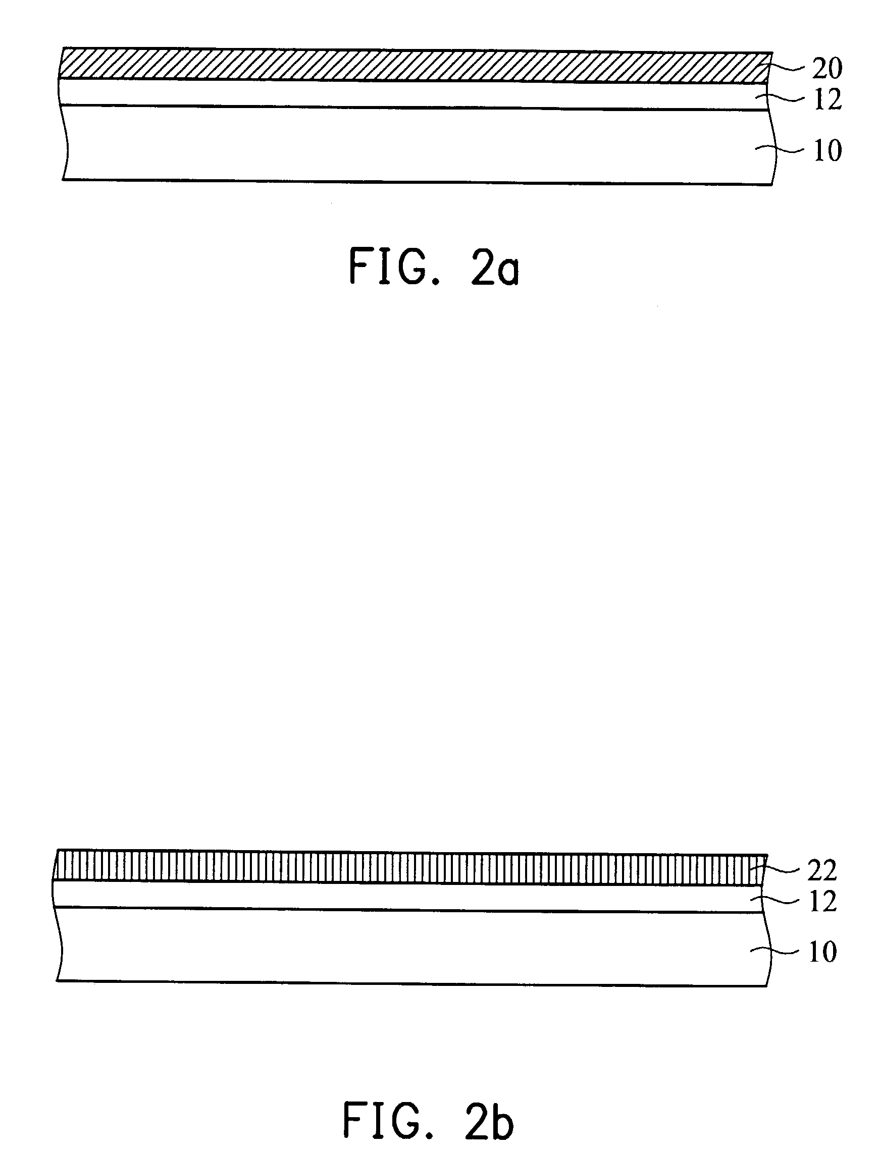
[0018]The present inventive cleaning is suitable for various silicon materials, including mono-crystalline silicon wafer, amorphous silicon, and polysilicon. For example, the present invention is suitable for cleaning mono-crystalline silicon wafer, amorphous silicon, or polysilicon in the semiconductor IC fabrication process, and amorphous silicon or polysilicon in the TFT-LCD fabrication process.

[0019]FIG. 1 is a flowchart illustrating the cleaning process for an amorphous silicon layer in the polysilicon TFT fabrication process. FIGS. 2a to 2i are cross-sections illustrating the proc...


PUM

PropertyMeasurementUnit
Fractionaaaaaaaaaa
Percent by massaaaaaaaaaa
Concentrationaaaaaaaaaa

Abstract

A process for cleaning a silicon surface. First, a silicon surface is cleaned with an oxidant solution. Next, the silicon surface is rinsed with HF vapor or liquid and then with the silicon surface with hydrogen water or deionized water under megasonic agitation. Finally, the silicon surface is cleaned with an oxidant solution a second time. The present inventive cleaning process can be applied in thin film transistor (TFT) fabrication and the TFT obtained has higher electron mobility.

Description

BACKGROUND OF THE INVENTION[0001]1. Field of the Invention[0002]The present invention relates to a process for cleaning a silicon surface, and more particularly to a process for cleaning a silicon surface in the TFT fabrication process for a TFT-LCD.[0003]2. Description of the Prior Art[0004]In the semiconductor IC and TFT-LCD array fabrication processes, the result of cleaning a silicon material plays an important role in the ultimate quality of IC devices and TFT arrays.[0005]In the semiconductor IC fabrication process, Caros (H2SO4 / H2O2), SC1 (standard clean 1; NH4OH / H2O2) and SC2 (standard clean 2; HCl / H2O2) cleaning methods have been extensively used for cleaning silicon wafers. These cleaning methods produce good cleaning results, but suffer from requiring a large amount of chemicals, resulting in environmental problems and additional treatment costs. In addition, ozone and HF have also been used to clean silicon wafers. For example, in U.S. Patent Application Publication No. ...

Claims


Application Information

Patent Timeline
IPC IPC(8): H01L21/465C25F3/30H01L21/306H01L21/77H01L21/84H01L27/12
CPCH01L27/1214H01L21/02052H01L27/127
Inventor PENG, CHIA-TIENSUN, MING-WEI
Owner AU OPTRONICS CORP
Why Eureka
Try Eureka